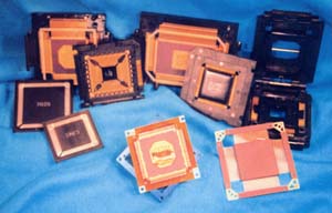
Successful Projects
Hughes Aircraft
Particle Interconnect - Hughes 1989 Fire Finder MCM

Particle Interconnect - Hughes Aircraft 1988 joint venture in Known-Good-Die
Resulting in a supercomputer assembled with Known-Good-Die in 2" x 4" x .1".
Science/Scope 1989 Hughes Aircraft Company:
"A new technique for packaging large-scale integrated circuit (IC) chips will permit much denser packaging on the substrate than previously possible. High-density multichip interconnect (HDMI) technology, being developed by Hughes, is designed to meet the needs of the next generation of VHSIC II hybrid circuits, which require dense packaging with no signal degradation at frequencies over 100 MHz. HDMI packaging achieves these results using a multi-layer substrate, a polymer dielectric highly suited to fine line metallization processing, and lithography techniques capable of producing 10-micron line widths. The technology is expected to be used in radar, sensing, tracking and guidance programs."
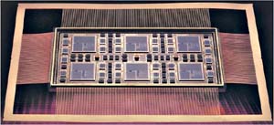
"The Data Memory Structure (DMS) multichip module is a very high speed cache memory system, switchable at high speed, to either of 3 input or output ports."
"HDMI can accommodate six 129K gate arrays (.640x.640 mil/die, 550+ pads/die; total 750,000 gates and 3,300 pads), 52 capacitors, and 24 - 15 nsec SRAM (32+ pads/die; total 750+), interconnected (using 70+ mil wire bond alleys) on a 2" x 4" = 8 in2 substrate having 368 I/O's."
"Performance of high speed circuits is also enhanced with low K polyimide dielectric used in the HDMI multilayer thin film (solder sealed ceramic leaded package) structure."
(All components tested/burned-in/speed sorted using PI resulting in 15+% yield improvement over production parts. Die price set at $5,000@ x 6 = $30,000, therefore DMS price >$100,000@)
PI's proposed removable die MCM-L/D/C to Hughes Aircraft.
Proposed to purchased a wafer for a total of $1,000 which was comprised of 300 die (5K gates/die .275 x .275 in.2/die, 180 pads/die for a total of 1,500,000 gates and 54,000 pads) interconnected on a 4" x 6" = 24 in.2 substrate. 50 mil pitch array yielded up to 9,600 I/O's.
Cost is further reduced by common low K polyimide multilayer PCB using 6+ mil pitch traces.
Environmental sealing of each die would also produce better reliability and upgradeability.
Particle Interconnect - Hughes Aircraft 1988 joint venture
Burned-in at 125 ° C for 168 hours.
 |
 |
| 15 mil pitch, 188 lead, JEDEC Standard TAB test socket with 50 MHz high level D.U.T. tester. | 15 mil pitch, 188 lead, JEDEC Standard TAB test socket. |

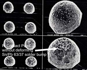
0.015" pitch OLB (Outer Lead Bond) - 0.006" pitch ILB (Inner Lead Bond) TAB (Tape Automated Bonding) tested/burned-in/speed-sorted.
- Excise line for flip chip mounting of TAB frame into finished MCM.
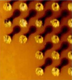
- Particle Interconnect ILB contact point onto 129k gate array.
Sandia Lab
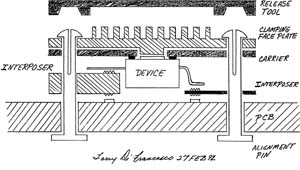
Particle Interconnect - Sandia Lab Known Good Die (KGD)
Known-Good-Die probe/burn-in. Proof of removable die MCM-L/D/C.
- 0.030" pitch 19x19 miniBGA.
- Burn-in at 125 ° C, 168 hours.
- 0 failures, 100+ runs, no deformation.
 |
 |
| 0 failures, 11 runs shown above. | Particle Interconnect surface mount BGA socket. |
 |
 |
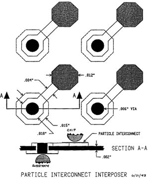
| Particle Interconnect - Sandia mBGA interposer schematic. | Sandia mBGA interposer |
Various projects
Particle Interconnect successful projects
Alternative Particle Interconnect lead frames vs. standard packages
Field replacable socket vs. nonfield replacable packages
 |
 |
| Field replacable socket diagram. |
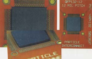
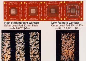
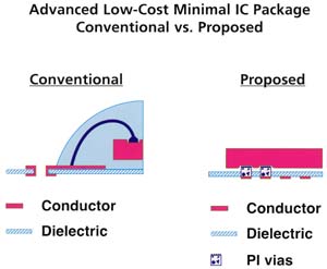
Particle Interconnect Package (PIP)
Advanced low-cost minimal IC package.
 |
 |
| QFP 132 lead, 0.012" pitch OLB (Outer Lead Bond). | Leadframe / Chip-On-Board socket & carrier. |
|
 |
Particle Interconnect MCM-L membrane test fixture
| PI used on flex-circuit material to form a translator bare-board test fixture. The translator is constructed by using a simple two-sided, plated-through-hole, printed circuit board (PCB), which is coated with PI on both-sides. The translator PCB accommodates the difference between off-grid test points of the unit under test (UUT) and the universal grid of the board test system. The bottom side matches up with the testers on-grid pads. Traces from the bottom side connect to the top side with plated-through holes. The translator PCB becomes the test fixture. |

0.010" pad, 0.015" pitch, 0.004" compliance. |
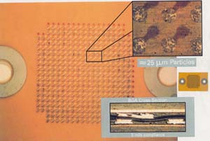
Particle Interconnect bare board membrane test fixture
| The 0.020" pitch board (see insert) with more than 2400 test points and 2000 PCB has been tested with a single bareboard membrane test fixture. |

|
Particle Interconnect - Cray J90 repackaging
Particle Interconnect, enabled the repackaging of the Cray J90 Vector Processor, by increasing connector density by about 100 times while maintaining ultrahigh speed signal integrity.
Reducing Cray form factor using PI