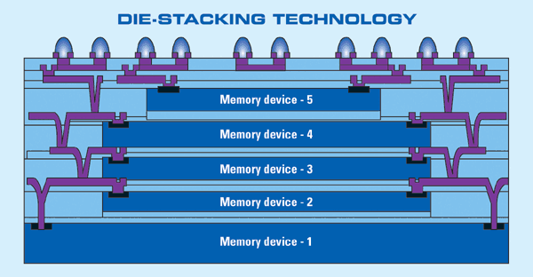
Particle Interconnect Stacked Die / Wafers
- Removable / reassemblable stacked die package
- Stacked wafers
- Products
- System In a Package (SIP)
- Competing non-remateable 3-D IC interconnects
- Reference
- DARPA 3D IC
Removable / reassemblable stacked die package
Removable / reassemblable stacked die package using Particle Interconnect
Patent 5,471,151 using existing die without modification. Unlike 3D wire bond die sizes are not important. Since dies are bonded at room temperature there is no induced thermal-mechanical stress.
 |
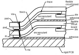 |
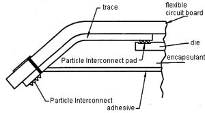
Flex circuit interposers
| Connecting two die. | Connecting several die. |
 |
 |
| 0.030" pitch 19x19 miniBGA socket. | 0.050" pitch, 15x15 through-hole BGA socket. |
Heat exchanger
- Cooling capacity: Demonstrated > 5000 W/cm2.
- Stress-free direct contact with die.
- Made of stacked electroformed layers with high thermal capacity microchannels.
- Microchannels have laminar flow, with the enhanced heat transfer coefficient inversely proportional to the width of the channel (heat transfer coefficient increases, as width decreases).
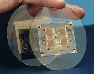
Stacked wafers
Silicon-on-sapphire IC mounted on sapphire wafer
Stacked two 3" sapphire wafers. 0.001" line, 0.001" space, with integrated decoupling capacitor, and integrated active substrate in 1982, using specially developed sputtered fluxless hermetic interconnect.
 |
 |
| Wafers before stacking | Close up |
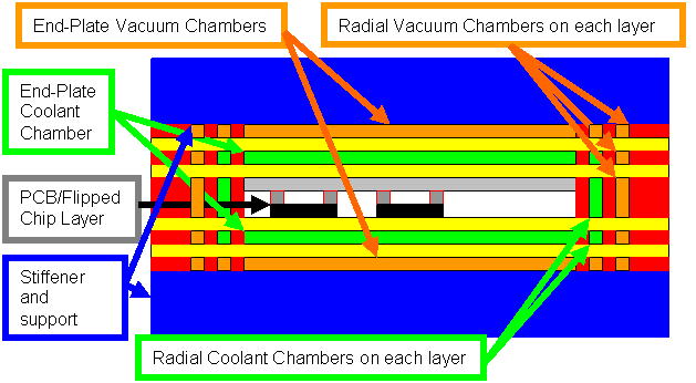
Cyrogenic cooled vaccum isolated stacked wafers
Stacking of vacuum chamber, coolant chamber, PCB/MCM, and flipped chips.
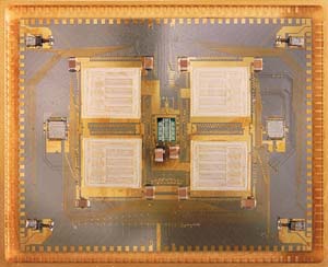
Products
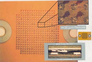
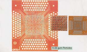
Particle Interconnect package
Advanced low-cost minimal IC package.
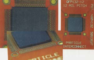 |
 |
| QFP 132 lead, 0.012" pitch OLB (Outer Lead Bond). | Leadframe / Chip-On-Board socket & carrier. |
|
 |
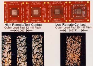
Particle Interconnect impression

Surface of PLCC J-Lead after 30,000 insertions. Surface finish of lead passed steam aging test.
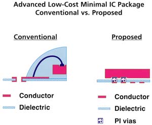
Remateable interposer
Inexpensive remateable and flexible interposer for through-silicon vias.
How to make through-silicon vias
Tru-Si Technologies Through-Silicon Vias
... The contact holes are made in the front side of the wafer, and an insulating layer of oxide is added to separate the silicon from the metal. After all front side processing is over, the wafer is simply thinned until the contacts are exposed. The ADP process etches the oxide so the metal is exposed, but it etches the silicon faster, so that the silicon remains insulated from the contacts in a very robust process.
Flash animation:
Removable / reassemblable die Multichip Module - L/D/C
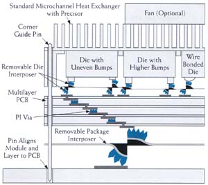
- Low-cost heat exchanger designed for modular dissipation needs.
- Removable / reassemblable die locator (precisor) aligns all die on 0.010" edge-to-edge mosaic tile pattern of silicon.
- Precisor is accurately aligned by corner guide pins in heat sink.
- Removable / reassemblable die PI interposer sockets die to PCB and spring loads die against heat sink.
- Interposer is accurately aligned by corner guide pins in heat sink.
- Removable / reassemblable die PI interposers with 0.001" - 0.008" travel on 0.001" - 0.030" pitch are available.
- Removable / reassemblable multilayer PCB interconnects all die together with controlled impedance from die pad to die to pad.
- PI vias between laminate layers allow 0.002" "blind" vias by punching through adhesive layer during lamination.
- PCB is accurately aligned by corner guide pins in heat sink.
- Removable package PI interposer sockets package to PCB and spring loads package to PCB.
- MCM is accurately aligned and held to PCB by corner guide pins for manual or automatic insertion.
- Package interposers with 0.08"-0.020" travel on 0.010"-0.050" pitch with either peripheral or array patterns available.
- Die are removable by simply unstacking layers.
- Both bumped and wire bond die pads are mixable.
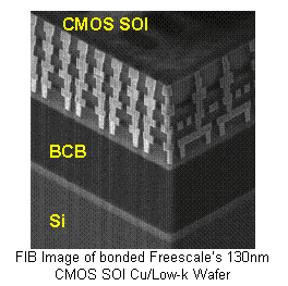
Competing non-remateable 3-D IC interconnects
Competing technologies are expensive and can not be disassembled and reassembled to remove defective parts.
Philip Garrou, MCNC Research & Development Institute, Research Triangle Park, N.C. -- 2/1/2005
...
3. Chip-in-polymer processes, such as that shown, have been developed by IMEC, Fraunhofer-Berlin and Fujitsu, among others. In such technologies, chips are thinned, embedded and interconnected in a thin-film/polymer matrix.
...
Wafer-to-wafer stacking is most practical for high-die-yielding individual wafer layers. Die-to-wafer bonding, where known good die (KGD) can be selected and bonded to KGD on the base wafer, is best suited for lower-yielding wafer layers.
...
A major limitation of the 3-D technology is alignment (best case now ±1-2 um), which currently limits this technology to global interconnect.
...
...
4. In the Fraunhofer-Munich process, KGD are remounted on a handle wafer and transferred all at once under pressure to the bottom wafer. This allows reflow of all the chips at once. When the eutectic bond is made, no further processing need occur on the top chip, thus eliminating exposure issues on the now non-planar surface.
...
So where does 3-D technology stand today? Remaining 3-D technology issues include:
. CAD tools for 3-D design, which are not widely available and not understood by a majority of design engineers.
. Thermal dissipation of heat from the stack.
. Yield that is exacerbated in wafer-to-wafer, stacking the need for common die size wafer-to-wafer alignment limitations, which has not yet achieved ± 1 um.
. Thermal-mechanical stresses induced by the post-device processing.
...
- Aligned Wafer Bonding for 3-D Interconnect
- RTI International 3-D Integration and Electronic Packaging
- Tru-Si Technologies Thru-Silicon Interposer
- Tru-Si Technologies Stacking
- 3D IC Industry Summary
- Rensselaer Polytechnic Institute's Center for Integrated Electronics
3D wirebond
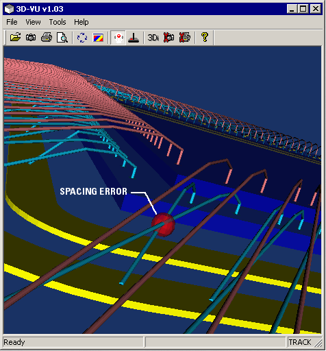
Cadence Allegro Package Designer 3D modeler
Reference
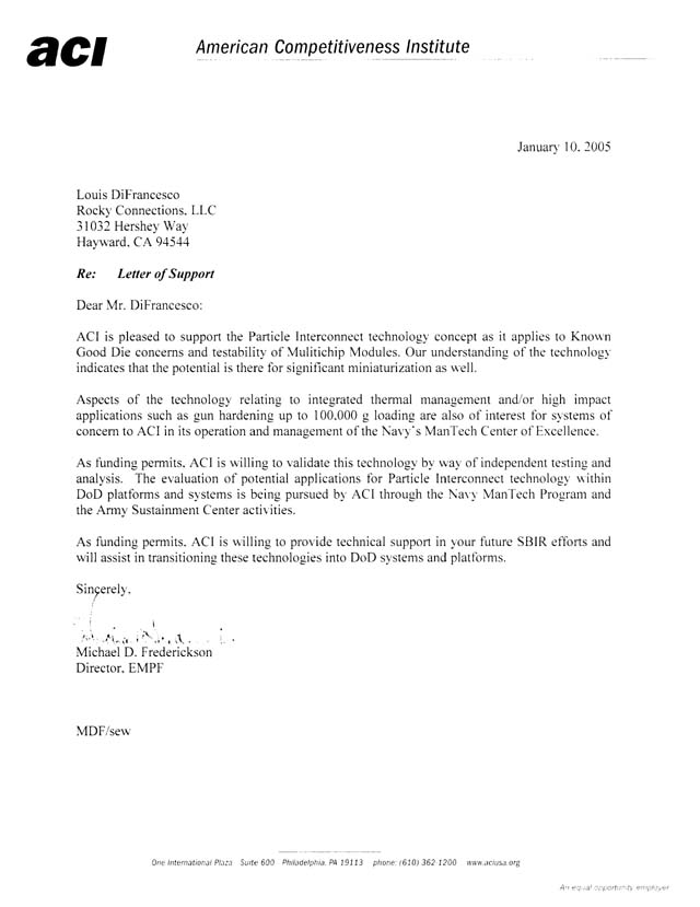
- The American Competitiveness Institute (ACI)
- The Electronics Manufacturing Productivity Facility (EMPF)
- Navy ManTech Manufacturing Technology Program
The American Competitiveness Institute (ACI) is a scientific research corporation dedicated to the advancement of electronics manufacturing processes and materials for The Department of Defense and industry. The company operates the U.S. Navy’s Center of Excellence in Electronics Manufacturing (Electronics Manufacturing Productivity Facility - EMPF), and the U.S. Army’s Electronics Sustainment Center (AESC). The EMPF focuses on the development, application and transfer of new electronics manufacturing technology by partnering with industry, academia and government centers and laboratories in the United States in order to maximize available research capabilities at the lowest possible cost. The AESC supports legacy systems with electronics technology upgrades by inserting commercial off the shelf (COTS) components into existing designs to enhance performance and reliability, reduce costs, and to mitigate component obsolescence issues. ACI also provides training, consulting, testing, analysis, and engineering services to the electronics industry.
EMPF is the U.S. Navy's National Center of Excellence dedicated to advancing the state-of-the-art in electronics and increasing domestic productivity in electronics manufacturing.