Papers on Particle Interconnect
- Mini BGA: Pad and Pitch Ease Die Test and Handling
- Particle Interconnect - Sandia Lab mBGA KGD packaging solution
- Removable die Multichip Module - L/D/C
- mini Ball Grid Array (mBGA) Technology
- mBGA Technology Overview
- Particle Interconnect: A New Interconnect Technology
- Socketing Chip-On-Board to a Multichip Module Using Particle Interconnect
- Particle Interconnect (PI) Technology, What Can It Do For You
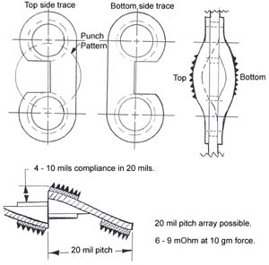
- Controlled impedance to lead of package
- Process cost comparison
- Particle Interconnect - Cray J90 repackaging
- Particle Interconnect - ACI
- Moving Toward the Transparent Connector
Mini BGA: Pad and Pitch Ease Die Test and Handling
by Rajen Chanchani, R. Keith Treece, Paul Dressendorfer
Advanced Packaging, May/June 1995
Flip-chip technology offers two main advantages over wirebond or TAB technologies: more I/Os can be accommodated on an area array with a larger pad pitch than with peripheral pads, and the dice can be flip-chip attached in proximity to achieve a higher circuit density. However, the following die-related issues must be addressed:
- Dice must be available in a flip-chip format. Dice designed with an area array of pads or bumps for flip-chip attach are ideal, but wide availability in this format is probably years away.
- Traditional flip-chip (C4) attachment uses relatively closely spaced solder bumps (0.008 - 0.010" pitch) requiring more expensive pick-and-place machines with tighter placement capabilities than those for standard SMD attachment.
- Bare chips must be available as known good dice (KGD) i.e., fully tested and screened for reliability.
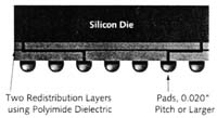 Figure 1. Cross-section of the mBGA. Conversion from peripheral to array-type I/Os permits bumps 0010" dia. on 0.020" pitch or larger.
Sandia National Laboratories has developed a minimally packaged die technology called mini ball grid array (figure 1) that addresses these issues. The mBGA features a flip-chip die with peripheral pads redistributed to an area array of pads 0.010" or larger in diameter with a minimum pitch of 0.020". mBGAs can be closely tiled together on a substrate to yield a very-high-circuit-density multichip module (MCM). The larger pad size and pitch of the mBGA not only facilitates die testing (to obtain KGD), but also cost-effective assembly using standard surface mount equipment and processes.
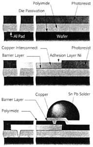 Figure 2. Stages of mBGA fabrication. Typical die size is 0.413 (side).
Description
In mBGAs, peripheral pads on a silicon die are redistributed to an area array using two polyimide di-electric layers. Standard photomask, etch, sputter and plate wafer processes are employed (figure 2). To date, various die types, including memory, ASICs, digital signal processor, microcontroller and several different test chips have been processed into mBGAs. A survey of ICs presently in use at Sandia showed that an array pitch of 0.030" was adequate for memories and processors. However, for pad-limited dies such as ASICs, an array pitch of 0.020" was required. As die sizes and peripheral die pad pitches continue to shrink, it may be necessary to reduce the mBGA array pitch below 0.020". Smaller array pitches, however, will burden the follow-on activities of die testing, die-to-substrate attachment and substrate routing.
MCM Test Vehicle
The MCM test vehicle, developed to evaluate the thermal and reliability performance of the mBGA assemblies, measures 1.26" and has four mBGA dice. Three are assembly test chips and the fourth is a daisy chain test die (figure 3). All have diagnostic features useful in characterizing the packaging technologies such as thermal performance and continuity of flip-chip bonds. The dice feature a total of 863 I/Os and the module has 239 peripheral I/Os. The silicon density (total dice area to total substrate area) is 66 percent and the interconnection density (total component and module I/Os to total module area) is 694 I/Os/in2, making the module a very-high-circuit-density MCM.
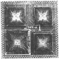 Figure 3. Four mBGA test chips feature 863 chip I/Os with 239 additional around the substrate's perimeter.
Test Fixtures
mBGA test fixture KGD can be obtained by individually testing the chips in a universal die carrier (figure 4). An alumina carrier substrate has a standard 20 x 20 PGA (0.100" pin pitch) on the bottom connected to a top pad array of gold bumps, 0.003" high on 0.030" pitch (0.020" pitch for the ASIC). Two threaded stainless steel pins, accurately placed with respect to the pads, position the spacer and the mBGA die in the carrier as well as clamp it in the carrier. The large size of the mBGA pads permits easy alignment to the pads on the carrier. The interposer, placed between the die and the carrier arrays, is a key element of the carrier in that it provides the electrical connection between the mBGA and the carrier. Two types of interposers have been successfully used: a Z-axis elastomer sheet and a 0.002" thick polyimide sheet with gold-coated diamond particle [Interconnect] embedded pads. For an effectively functioning interposer, a clamping force between mBGA and carrier is required.
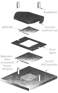 Figure 4. Univeral mBGA die carrier. Once a chip is seated, it may be tested and burned-in as a conventional PGA component, but yielding a "known good die."
Once an mBGA die has been seated in a carrier, it may be tested and burned-in as a conventional PGA part. Since the carrier presents a common footprint (20 x 20 PGA) for all die types, Sandia has designed universal load boards for an HP 82000 tester and burn-in boards for an AMT M300 burn-in system. These boards can be personalized for a particular die type by jumpering appropriate pins.
The MCM test fixture accommodates an air-cooled heat sink (providing a thermal path from the top surface of the dice) or liquid-cooled heat sink (providing a thermal path through the substrate). In an investigation of different cooling schemes, a special HP 82000 load board accommodates the assembled module with either type of heat sink. The module is electrically connected to the load board with a Z-axis elastomer. The load board and the module, with or without the heat sinks, are clamped together by a set of screws. Results of their cooling effectiveness are shown in figure 5.
Results of KGD Tests
All dice types haye been tested in mBGA carriers on IC testers. These tests included DC parameters, AC timing and maximum frequency tests using full functional vector sets. A total of about 300 mBGA dice were tested at frequencies up to 100 MHz, over the voltage range 4.5 to 5.5 V, and over the temperature range 0 ° to 70 ° C. (Some dice were characterized over the range -30 ° to 130 ° C.) Over these ranges. mBGA carrier data have agreed closely with corresponding test data from wire-bonded, commercially packaged parts. Although the die carriers did not have controlled-impedance interconnect, they could be so constructed for testing high speed (over 100 MHz) dice.
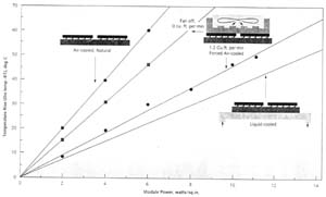 Figure 5. Thermal performances of mBGA on silicon MCM-D substrate with various cooling schemes.
After a thorough electrical test, dice were given a 168-hour monitored burn-in at 125 °. To date, over 100 dice have completed burn-in with negligible effects on the mBGA or carriers. Some carriers have seen over 1,000 hr at 125 ° C and appear robust under this condition. Except for the Z-axis elastomer inter-posers, which were replaced after each 168-hour cycle, none of the carrier parts, including diamond particle interposers, has shown degradation.
Results of mBGA Assembly Tests
The main reliability concern in mBGA assembly is thermal fatigue cracking of the flip-chip joints caused by the CTE mismatch between mating materials during thermal cycles. Previous studies on the reliability of C4 joints are encouraging: No flip-chip joint failure has been noted in any of the millions of C4 joints in the field.2 Although the mBGA flip-chip joints are conceptually similar to C4 joints, there is a significant difference in their geometries. C4 joints are 0.004 to 0.005" dia. on 0.008 to 0.010" pitch, whereas mBGA joints are 0.010 to 0.015" dia. on 0.020 to 0.030" pitch. The aspect ratio of joint diameter-to-height is approximately 1 for a C4 joint and about 2 to 3 for mBGA joint. The effects of geometrical differences between C4 and mBGA joints on the reliability are not clearly known.
To date, thermal cycle tests have been performed on mBGA dies attached without underfill to MCM-D substrates of silicon and alumina. All substrates had five layers of polyimide dielectric and metal, including power and ground planes. mBGA dies were attached with both 60/40 and 5/95 Sn/Pb solders and with conductive epoxy. Temperature cycles between 0 °, and 100 ° C were 30 min in duration with transition times of a few seconds. During cycling, flip-chip joint integrity was periodically monitored via electrical continuity tests. All assemblies survived 1000 thermal cycles.
ACKNOWLEDGEMENTS
The authors acknowledge APTOS for fabricating the mBGA dies and silicon substrate. Microelectronic center of North Carolina for fabricating ceramic substrates. Texas Instruments for assembling the module and 3M Co. for conductive adhesive attaching the mBGA dies to the substrate. Acknowledgments are also due to Scott Bieber. John Baca. Gerald Hash and Anthony Griego of Sandia National Labs for their help in design and testing of the parts.
REFERENCES
1 J. N. Sweet, M. R. Tuck. D. W. Peterson and D. W. Palmer, "Short and Long Loop Manufacturing Feedback Using a Multisensor Assembly Test Chip," IEEE Trans. on Components, Hybrids and Manufacturing Technology. 14. 529-535 (1991).
2 A. P. Ingraham, J. M. McCreary and J. A. Varcoe. "Flip Chip Soldering to Bare Copper Circuits." IEEE Trans. on Components. Hybrids and Manufacturing Technology. 13. 656-660 (1990).
RAJEN CHANCHANI is senior staff member. KEITH TREECE is distinguished member of technical staff, and PAUL DRESSENDORFER is manager of MCM applications department at Sandia National Laboratories. P.O. Box 5800. M/S 1073. Albuquerque. N.M. 87185-1073: (505) 844-3482; Fax (505) 844-8480.
Interposer detail
 |
 |
| (a) Particle Interconnect - Sandia mBGA interposer schematic | (b) Sandia mBGA interposer |
Particle Interconnect - Sandia Lab mBGA KGD packaging solution
Known-Good-Die probe/burn-in. Proof of removable die MCM-L/D/C.


Particle Interconnect - Sandia Lab Known Good Die (KGD)
Known-Good-Die probe/burn-in. Proof of removable die MCM-L/D/C.
- 0.030" pitch 19x19 miniBGA.
- Burn-in at 125 ° C, 168 hours.
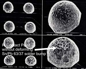
- 0 failures, 100+ runs, no deformation.
 |
 |
| 0 failures, 11 runs shown above. | Particle Interconnect surface mount BGA socket. |
|
|
| Particle Interconnect - Sandia mBGA interposer schematic. | Sandia mBGA interposer |
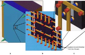
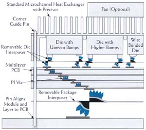
Removable die Multichip Module - L/D/C
|
|
 |
 |
| Removable die MCM | Louver contact |
- Low-cost heat exchanger designed for modular dissipation needs.
- Removable die locator (precisor) aligns all die on 0.010" edge-to-edge mosaic tile pattern of silicon.
- Precisor is accurately aligned by corner guide pins in heat sink.
- Removable die PI interposer sockets die to PCB and spring loads die against heat sink.
- Interposer is accurately aligned by corner guide pins in heat sink.
- Removable die PI interposers with 0.001" - 0.008" travel on 0.001" - 0.030" pitch are available.
- Removable multilayer PCB interconnects all die together with controlled impedance from die pad to die to pad.
- PI vias between laminate layers allow 0.002" "blind" vias by punching through adhesive layer during lamination.
- PCB is accurately aligned by corner guide pins in heat sink.
- Removable package PI interposer sockets package to PCB and spring loads package to PCB.
- MCM is accurately aligned and held to PCB by corner guide pins for manual or automatic insertion.
- Package interposers with 0.08"-0.020" travel on 0.010"-0.050" pitch with either peripheral or array patterns available.
- Die are removable by simply unstacking layers.
- Both bumped and wire bond die pads are mixable.
mini Ball Grid Array (mBGA) Technology
by
Rajen Chanchani, R. Keith Treece, Paul Dressendorfer
Multichip Module Applications Department
Sandia National Laboratories
ABSTRACT
Sandia National Laboratories has developed a minimally packaged die technology, called mini Ball Grid Array (mBGA) as shown in Figure 1. The mBGA is a flip chip die, obtained by redistributing peripheral pads in existing dies to an area array of pads 10 mils or larger in diameter with a minimum pitch of 20 mils. mBGAs can be closely tiled together on a substrate to yield a very high circuit density multichip module (MCM). The large pad size and pitch of the mBGA not only facilitates die testing to obtain "known good die", but also allows cost-effective flip chip assembly using standard surface mount equipment and processes. This paper describes the mBGA technology and the test vehicle multichip module, and reports preliminary results on the die test and burn-in, thermal performance and reliability studies.
INTRODUCTION
Flip chip technology offers two main advantages over wire bond or TAB technologies. First, a significantly higher number of die I/Os can be accommodated on an area array with a. larger pad pitch for flip chip attach than can be done with peripheral pads. Second, the dies can be flip-chip attached in close proximity with each other to achieve a higher circuit density. However, the following die related issues need to be addressed before using flip chip technology.
- Dies must be commercially available in a flip chip format. It is likely that most commercial dies for next several years will be available from the manufacturers only with peripheral pads for wire bonding. Although these pads could be solder bumped for direct flip chip attach, the bump spacing will be very small (smaller than traditional flip chip (C4) bump spacings). Ideally, one would want die designed with an area array of pads for flip chip attach, but wide availability of this format is many years away.
- Traditional flip chip (C4) attachment uses relatively closely spaced solder bumps (8-10 mil pitch) requiring more expensive pick and place machines with tighter placement tolerances than those utilized for standard SMT component attachment.
- Bare dies must be available as Known Good Die (KGD), fully tested and reliability screened.
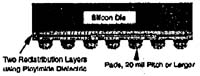 Figure 1. Schematic Drawing of mini Ball Grid Array (not to scale)
Sandia National Laboratories has developed a minimally packaged die technology, called mini Ball Grid Array (mBGA). shown in Figure 1, that resolves all these three issues. The mBGA is a flip chip die, obtained by redistributing peripheral pads in existing dies to an area array of pads 10 mils or larger in diameter with a minimum pitch of 20 mils. mBGAs can be closely tiled together on a substrate to yield a very high circuit density multichip module (MCM). The large pad size and pitch of the mBGA not only facilitates die testing to obtain "known good die", but also allows cost-effective flip chip assembly using standard surface mount equipment and processes.
This paper describes the mBGA technology and the test vehicle multichip module, and reports preliminary results on the die test and burn-in, thermal performance and reliability studies.
DESCRIPTION OF mBGA
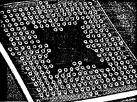 Figure 2a. ASIC mBGA with 275 pads on .020" pitch. Die size = .413" square.
In mBGAs, peripheral pads on a silicon die are redistributed to an area array using two polyimide dielectric layers by post processing silicon wafers. Standard photo-mask, etch, sputter and plate wafer processes are used. Sandia has worked with APTOS (Milpitas, CA) and General Electric (Schenectady, NY) to develop mBGA wafer processing capabilities. Micrographs of a mBGA die are shown in Figure 2. Even though the specific processes from the two vendors differ somewhat, the general process flow is shown in Figure 3. To date, seven different die types, listed in Table 1, have been processed into mBGAs. A 30 mil pad array pitch and 2 mil lines/spaecs/vias were used for all die except the ASIC. As die peripheral pad pitch is reduced to 5 mils and below, more aggressive mBGA design rules are required as illustrated in the ASIC, which has about 300 peripheral pads on 5 mil pitch. The ASIC die required 20 mil array pitch. Reducing the array pitch below 20 mils would further burden the follow-on activities such as die testing, die-to-substrate attachment and the substrate routing. For all ASIC dies surveyed to date, an area pad array of 20 mil pitch or higher was found to be adequate to allow redistribution of all peripheral pads within the die area.
 Figure 2b. Magnified view showing solder bumps and interconnect metalization.
The terminations on the I/O pads are cither gold, 40/60 or 95/5 Pb/Sn solders. Thus, mBGAs can be either solder or conductive adhesive attached to the substrate. Since the pad size, pitch and metallurgy of the mBGA is similar to other surface mount component, its testing and alignment/attachment processes are also similar.
DESCRIPTION OF MCM TEST VEHICLE
The MCM test vehicle, shown in Figure 4, was developed to evaluate the thermal and reliability performance of the mBGA assemblies. The module size is 1.26" square and it has a total of 4 mBGA dies. Three dies are Sandia's ATC03 assembly test chips[1] and the fourth die is a X40 daisy chain test die (see Table 1). All dies have diagnostic features useful in characterizing the packaging technologies. These four dies have a total of 863 I/Os and the module has 239 peripheral I/Os. The silicon density (total die area/total substrate area) is 66% and the interconnection density (total component and module I/Os/total module area) Is 694 I/Os per sq. inch, which makes this module a very high circuit density MCM.
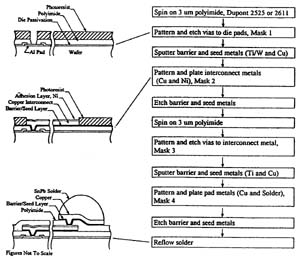 Figure 3. Typical mBGA fabrication process.
ATCO3 die
ATC03 is one of the dies from a family of Sandia's Assembly Test Chips. It contains temperature and strain sensors, triple tracks for corrosion studies and heaters. Each die is 0.25 inch square. To simulate a larger die, we used an ATC03 quad, 0.5" square. obtained by dicing a cluster of four dies from a wafer. ATC03 quad was used to study the thermal performance of mBGA dies.
X40 die
X40 is a blank die with 191 peripheral pads, all of which are daisy chain connected through the substrate. This die was used to test the continuity of flip-chip bonds in thermal fatigue tests.
Substrate
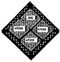 Figure 4. Multichip Module test vehicle
The primary substrate material used in testing to date are silicon and alumina with five metal/polyimide dielectric layers. These layers are one power, one ground, two signal planes and a top pad layer. The metal layers are made up of titanium, tungsten, copper and nickel. In the top pad layer, flip-chip pads are terminated with either gold, 40/60 or 95/5 Pb/Sn solders. The peripheral pads are finished with gold in all substrates. Laminate (MCM-L) substrates are also being fabricated for future evaluation.
mBGA die-to-substrate attachment
mBGA dies were attached to the substrate by either (i) 95/5 solder (high temperature reflow), (ii) 40/60 solder (low temperature reflow), or (iii) 3M's S40B developmental conductive adhesive. The silicon substrate modules were solder assembled at Texas Instruments Dallas, TX). and conductive adhesive attached at 3M (St Paul. MN). In the high temperature reflow, the pre-fluxed assembly was heated to 355 ° C in a reducing atmosphere and in the low temperature reflow, the pre-fluxed assembly warn heated to 235 ° C in air. The S40B conductive adhesive sheet was used in assemblies with gold pads and was cured at 180 ° C to 190 ° C for 3 minutes under a pressure of about 115 lbs per die.
TEST FIXTURES
mBGA test fixture
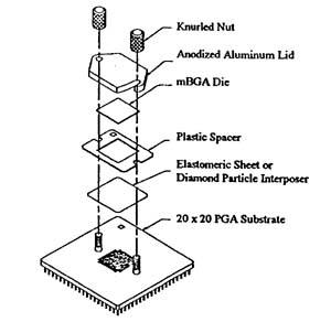 Figure 5. Univeral Die Carrier
mBGA "known good dies" can be obtained by individually testing the dies in an universal die carrier (Figure 5). An alumina carrier substrate has a standard 20 x 20 PGA (0.1" pin pitch) on the bottom connected to a top pad array of gold bumps, .003" high on .030" pitch (20 mils pitch for the ASIC). Two threaded stainless steel pins, accurately placed with respect to the pads, position the spacer and the mBGA die in the carrier as well as clamp the die in the carrier. Since the size of the rnBGA pads is large, they are easily aligned to the pads on the carrier. A key element of the carrier is the interposer, placed between the die and the carrier arrays, that provides the electrical connection between the mBGA and the carrier. Two types of interposers have been successfully used: (1) a z-axis elastomer sheet, and (2) a .002" thick polyimide sheet with gold-coated diamond particle embedded pads. For an effectively functioning interposer, a clamping force between mBGA and carrier is required.
Once an mBGA die has been seated in a carrier, it may be tested and burned-in as a conventional PGA part. Since the carrier presents a common footprint (20 x 20 PGA) for all die types, Sandia has designed universal load boards for an HP82000 tester and burn-in boards for an AMT M300 burn in system. These boards can be personalized for a particular die type by jumpering appropriate pins.
 Figure 6. Different cooling schemas studied.
MCM test fixture
The MCM test fixture accomodates an air cooled heat sink, providing a thermal path from the top surface of the dies, or a liquid-cooled beat sink providing a thermal path through the substrate. We investigated different cooling schemes as shown in Figure 6. A special HP 82000 load board was designed to accomodate the assembled module with either type of heat sink. The complete board assembly for testing on HP 82000 is shown In Figure 7. The module is electrically connected to the load board with a z-axis elastomer. The load board and the module with or without the heat sink are clamped together by a set of screws.
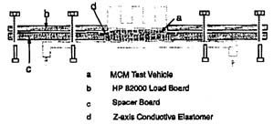 Figure 7. A test fixture for MCM test vehicle.
RESULTS
"Known Good Die" tests
To date all die types shown in Table 1 (except the SA3470 Microcontroller) have been thoroughly tested in mBGA carriers on HP 82000 IC testers. These tests included dc parameters, ac timing and maximum frequency tests using full functional vector sets. A total of about 300 mBGA dies were tested over the voltage range 4.5V to 5.5V, and over the temperature range 0 ° C to 70 ° C, Some dies were characterized over the range -30 ° C to 130 ° C. Over these ranges, mBGA carrier data have agreed closely with corresponding test data from wire-bonded, commercially packaged parts, as shown in Table 2 for maximum frequency (Pmax) tests. The die carriers used did not have controlled impedance interconnect, but could be so constructed for testing high speed (over 100 MHz) die.
After a thorough electrical testing, all dies were tested for a 168-hour, dynamic monitored burn-in test at 125 ° C. To date, over 60 dies have completed burn-in with negligible effects on the mBGA die or carriers. Some carriers have seen over 1000 hours at 125 ° C and appear robust under this condition. Except for the z-axis elastomer interposers which were replaced after each 168-hour cycle, none of the carrier parts, including diamond particle interposers, has [have] shown any degradation.
Thermal performance of mBGA
A primary concern in many MCM applications is the maximum power allowed and the type of thermal cooling scheme required. These factors directly affect module reliability and tbe overall system miniaturization. The thermal performance of mBGA on silicon MCM-D was experimentally determined. The module was powered through the heaters located in three ATC03 dies (refer to Figure 4). A minimum of 1 watt/ATC03 die or 3 watts/module power was initially provided and the die temperatures were noted using temperature sensing diodes on ATC03. Measurements were taken at power increments until a die temperature of 85 ° C or the current carrying capacity of the HP 82000 test circuit (18 watts/module) was reached. Twenty minutes before each reading were allowed for the module to reach steady state.
Figure 8. Thermal Performance of mBGA on silicon MCM-D substrate
This procedure was repeated for four cooling conditions (Figure 6), natural air-cooled (without heat sink), air-cooled heatsink with fan off (no air flow), air-cooled heatsink with fan on (forced air @ 1.2 cu. ft. per minute) and liquid-cooled heatsink. The results, power (watts/square inch) versus an average mBGA die temperature increase, are shown in Figure 8. With the natural air-cooled condition, the module is capable of dissipating maximum 6 watts per square inch before temperature rise of 65 ° C is reached. With either the forced air-cooled or liquid-cooled heatsinked module, the maximum power tolerated is well above 12 watts per square inch. There is a significant improvement in thermal performance of modules with air-cooled heatsink module over that of natural air-cooled (without heat sink). A further improvement, as expected. is seen with liquid-cooled module. In our experiment, the coolant (water at room temperature) flow rate through the heat sink was maintained at 0.5 litres per minute. Thermal performance will further improve by increasing the flow rate or decreasing the temperature of the liquid. These results can be extrapolated for real MCMs. For example, if we have a 2" x 2" module, we can input over 48 watts by using forced-air cooling (air-cooled heatsink with fan on).
No cooling augmentation is required if the power is less than 6 watts per sq. inch. For higher module power, either air-cooled or liquid-cooled heat sinks must be used. When the heat is dissipated from the top of the dies, an air-cooled heat sink must be used. When the thermal path is through the substrate, a liquid-cooled heat sink is recommended for high power applications because of the higher thermal impedance provided by polyimide layers on the die as well as on the substrate. These results are valid for silicon MCM-D technology similar to that used in this study and when heat is generated evenly on the module surface.
Reliability of flip-chip joints
The main reliability concern in mBGA assembly is thermal fatigue cracking of the flip-chip joints caused by thermal expansion mismatch between the mating materials during thermal cycles. Previous studies [2] on the reliability of C4 joints are encouraging. No flip-chip joint failure has been noted in any of the millions of C4 joints in the field. Although the mBGA flipchip joints are conceptually similar to C4 joints, there is a significant difference in the geometry. C4 joints are 4 to 5 mil diameter on 8 to 10 mil pitch, whereas mBGA joints are 10 to 15 mils diameter on 20 to 30 mil pitch. The aspect ratio of joint diameter to height is approximately 1 for a C4 joint and about 2 to 3 for a mBGA joint. The effect of geometrical differences between C4 and mBGA joints on the reliability are not clearly known. We have initiated a detailed study of mBGA joint reliability with only preliminary results presented here.
We have temperature cycled the mBGA assemblies listed in Table 3 from 0 to 100 ° C for 1000 cycles. Temperature cycles were 30 minutes in duration with transition times of a few seconds. During temperature cycling, we periodically monitored the flip chip joint integrity by performing electrical continuity tests. All modules survived 1000 cycles. The temperature range tested (0 to l00 ° C) is the thermal load typically found in consumer electronics.
CONCLUSIONS
mBGA, a minimally die packaging technology developed at Sandia, involves redistributing peripheral pads on silicon die to an area array pads with 20 mil pitch or larger using two rnetal/dielectric layers.
We have tested mBGAs in MCM using a test vehicle, which was specifically designed and fabricated for this purpose. The mBGA dies used in the test vehicle are an assembly test chip ATC03 and a daisy chained die, X40. The diagnostic features on these dies allowed us to evaluate the thermal and reliability performance of the module.
To date, we have tested MCM-D using silicon or alumina substrates with five layers of polyimide dielectric and metal conductors. For silicon MCM-D modules, no thermal enhancement is required if the power is less than 6 watts per sq. inch of module. For higher module power, up to about 12 watts per sq. in., either air-cooled or liquid-cooled heat sinks can be used. The assembled mBGA modules survived the preliminary reliability tests involving 1000 thermal cycles, from 0 to 100 ° C.
ACKNOWLEDGMENTS
The authors wish to acknowledge APTOS for fabricating the mBGA dies and silicon substrate, Microelectronic Center of North Carolina for fabricating ceramic substrates, Texas Instruments for assembling the module and 3M Co. for conductive adhesive attaching the mBGA dies to substrate. Acknowledgments are also due to Scott Bieber. John Baca, Gerald Hash and Anthony Griego of Sandia National Labs for their help in design and testing of the parts.
This work was performed at Sandia National Laboratories and supported by the U.S. Department of Energy under contract DE-AC04-94AL85000.
REFERENCES
1 J. N. Sweet, M. R. Tuck, D. W. Peterson and D. W. Palmer, "Short and Long Loop Manufacturing Feedback Using a Multisensor Assembly Test Chip," IEEE Trans. on Components, Hybrids and Manufacturing Technology, 14. 529-535 (1991).
2 A. P. Ingraham. J. M. McCreary and J. A. Varcoe, "Flip-Chip Soldering to Bare Copper Circuits," IEEE Trans. on Components, Hybrids and Manufacturing Technology, 13, 656-660 (1990).
TABLE 1. mBGA Processed Die Types
| Die Type | Description | No. of Pads | Pad Array Pitch |
| MT5C2568 | Micron Memory | 34 | .030" |
| PDSP16515 | Plessey DSP | 128 | .030" |
| LCA100106 | LSI Logic ASIC | 275 | .020" |
| SA3470 | Sandia Microcontroller | 52 | .030" |
| X40 | Xilinx Test Die | 191 | .030" |
| ATC03 | Sandia Assembly Test chip | 224 | .030" |
| ATC04 | Sandia Assembly Test chip | 35 | .030" |
TABLE 2. Fmax Test Data For mBGA and Commercial Packages
| Fmax at 0 ° C (MHZ) | Fmax at 70 ° C (MHZ) | ||||
| Dic Type | Package | 4.5 V | 5.5 V | 4.5 V | 5.5 V |
| MT5C2568 | mBGA | 72.5 | 80.6 | 67.6 | 75.7 |
| Commercial | 71.8 | 78.7 | 66.1 | 74.2 | |
| PDSP16515 | mBGA | 86.3 | 97.2 | 75.3 | 83.2 |
| Commercial | 88.0 | 98.9 | 77.3 | 85.0 | |
| LCA100106 | mBGA | 27.3 | 32.1 | 21.2 | 25.4 |
| Commercial | 25.6 | 30.8 | 20.0 | 24.1 | |
TABLE 3. Description of MCMs Used in Reliability Study
| Module # | Substrate | Die Pad | Substrate Pad | Joint Material | Passed / failed* |
| 29 | silicon | Gold | Gold | S40 B adh. | Passed |
| 43 | silicon | 60/40 solder | 60/40 solder | 60/40 solder | Passed |
| 39 | silicon | 60/40 solder | 60/40 solder | 60/40 solder | Passed |
| 13 | silicon | 60/40 solder | 95/5 solder | 60/40-95/5 solder | Passed |
| 47 | silicon | 95/5 solder | 95/5 solder | 95/5 solder | Passed |
| c14 | alumina | 60/40 solder | 95/5 solder | 60/40-95/5 solder | Passed |
* Temperature cycled, 0 to l00 ° C, l000 cycles. Module #47 ran for 700 cycles only, broke during handling.
mBGA Technology Overview
by
R. Keith Treece
Distinguished Member of Technical Staff
Sandia National Laboratories
Albuquerque, New Mexico
Abstract
A new die-level packaging technology, called mini Ball Grid Array (mBGA), is presented. This technology provides the smallest possible IC package, which is cost effective and relatively easy to test, burn-in, and assemble. Packaging cost estimates and Sandia's test strategy and experience for obtaining ''known good die" are also described.
Introduction
Ball grid arrays (BGA) are a relatively recent, exciting new IC package development which offers advantages over other SMT packages, such as: smaller footprint, improved electrical performance, and easier handling and assembly because of the robust nature and large pitch of the solder balls. However, even though BGA packages are often more than 2X smaller than pin-comparable QFPs, their footprint is still considerably larger than the die itself, often 4X-8X bigger. Flip chip die, such as IBM's C4, are optimally small and have other advantages of area array pads, but such die are not widely available and are challenging to test, assemble, and interconnect because of their small pad pitch (.25 mm, .010").
Figure 1a. ASIC mBGA with 275 pads on .020" pitch. Die size = .413" square.
Sandia Labs has developed over the past three years a minimally packaged die technology, called mini Ball Grid Array (mBGA), which has most of the combined advantages of BGA packages and flip chip die (Figure 1). mBGA is similar to BGA packaging technology in that it protects the active surface of the die and redistributes the peripheral die pads to an area array of bumped pads on relatively large pitch (.50 mm - .75 mm). The large pad pitch facilitates testing, assembly, and interconnection to the pads, and like C4 die, the mBGA package is no larger than the die itself.
This paper will describe the fabrication processes and give cost estimates for mBGA packaged die. Also, Sandia's strategy and experience w ith testing and burn-in of mBGAs will be presented, along with our plans for developing attachment and rework processes and for performing reliability assessments.
Figure 1b. Magnified view showing solder bumps and interconnect metalization.
mBGA Fabrication Process
Although the ideal source for die with area array pads would be directly from integrated circuit suppliers, most die for the next several years will probably have peripheral wire bond pads (Vardaman 1994). mBGA packages are fabricated by post processing conventional, wire-bond integrated circuit wafers using standard photo-mask, etch, sputter, and plate procedures. All die on the wafer are "packaged" at the same time. Sandia has worked with two suppliers to develop mBGA wafer processing capabilities: Aptos (Milpitas, CA.) and from General Electric (Schenectady, NY.). Even though their processes are somewhat different, the four mask process shown in Figure 2 illustrates the salient features.
Figure 2. Typical mBGA fabrication process Flow
To date, wafers for six different die types (Table 1) have been processed for use in MCM prototypes and for evaluation of mBGA processing, flip chip attach techniques. and die testing methods. A .75 mm (.030") pad array pitch and 50 um lines. spaces, and vias were used for all die except the ASIC. The ASIC die, which had nearly 300 peripheral pads on .005" pitch. required a .5 mm (.020") array pitch and 25 um vias to the peripheral pads. As die suppliers reduce the peripheral pad pitch below .005". it may become necessary to use more aggressive design rules for mBGA processing. These could include reduced line width and space, additional redistribution layers, and a reduced array pitch. Reducing the array pitch below .5 mm, however, adds more burden to follow-on activities such as testing the die, attaching it to the substrate, and routing the substrate.
TABLE 1. mBGA Processed Die Types
| Die Type | Description | No. of Pads | Pad Array Pitch |
| MT5C2568 | Micron Memory | 34 | .030" |
| PDSPl6515 | Plessey DSP | 128 | .030" |
| LCA100106 | LSI Logic ASIC | 275 | .020" |
| SA3470 | Sandia Microcontroller | 52 | .030" |
| XC4010 | Xilinx Test Die | 191 | .030" |
| ATC03 | Sandia Assembly Test Chip | 224 | .030" |
mBGA Packaging Costs
The post wafer processing costs for producing mBGA die include fixed, non-recurring costs for mask layout and procurement, and setup charges for process parameter calculations. Sandia's experience shows that for 150 mm diameter wafers, these NRE costs total about $ 10k per wafer type. The processing cost per good mBGA die depends upon the number of die per wafer, the initial die yield, and wafer quantity. Die yields, due only to mBGA processing, of > 98% have been achieved. Assuming an overall 50% die yield, Table 2 shows Sandia's estimates for production costs on two die types: a low pin count microcontroller, and a high pin count ASIC. The decrease in cost with higher wafer quantity is based on Aptos' production experience with bumping wafers for TAB packaging. The 2k/month quantity estimates for mBGAs compare favorably to production cost estimates for BGA and PQFP packages, which currently are about 4 and 2 cents per pin, respectively (Derman 1994).
TABLE 2. Sandia Cost Estimates For mBGA Packaging
| Die Type | Die/Wafer | Good Die/ Wafer (50%) | Pads/Die | Wafer Quantity | Cost/Wafer | Cost/Good Die | Cost/Pad |
| uController | 300 | 150 | 50 | 1-10 | $800. | $5.33 | $0.11 |
| 2k/Mo. | $220. | $1.47 | $0.03 | ||||
| ASIC | 126 | 63 | 300 | 1-10 | $800. | $12.70 | $0.04 |
| 2k/Mo. | $220. | $3.50 | $0.01 |
mBGA Testing Strategy
Universal Die Carriers
Figure 3a. Univeral Die Carrier, Exploded View
The relatively large pad size and pitch on mBGAs allows the die to be easily aligned and contacted in universal die carriers, shown in Figure 3. Carriers with both .020" and .030" array pitches have been used successfully to test die at speed and over the temperature range -60 ° C to 130 ° C. The carrier substrates, used to date, are alumina ceramic with a standard 20x20 PGA (0.1" pin pitch) on the bottom connected to a pad array of gold bumps, .003" high on .020" or .030" pitch, on the top. For testing high frequency die (>200 MHz), planes could be added to the substrate to provide controlled impedance signal lines. Also, Sandia is working with a supplier to make low cost carrier substrates out of FR-4 material. Two threaded stainless steel pins are accurately positioned with respect to the pad array and bonded into place on the substrate. The pins accurately position the die spacer and provide a mechanism for clamping the mBGA die in the carrier. The plastic spacer is the only carrier piece which is unique to a particular die type. It's function is to center the die over the substrate array and to provide a positive stop so that the lid cannot be over-tightened on the die. The aluminum lid directly contacts the backside of the mBGA die, and can be finned (Figure 3b) to provide an effective heat sink.
 Figure 3b. Univeral Die Carrier With mBGA
A key element of the carrier is the interposer between die and carrier arrays. Two types of interposer have been used: z-axis elastomer sheets, and a membrane with gold-coated diamond particles on pads contacting the die solder bumps. The elastomer sheet provides a compliant interconnect which has worked well if the die bumps are clean, free of any flux residue, and at temperatures up to 100 ° C. Since the elastomer is soft, it does not abrade or penetrate any insulating films which may be present on solder bumps. Also, above 100 ° C we have observed erratic variation in contact resistance.
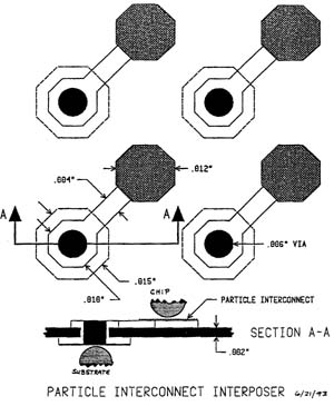
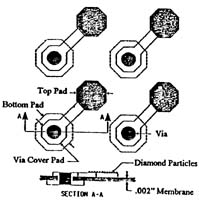 Figure 4a. Diamond Particle Interposer Design
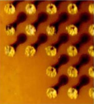
The diamond particle interposer is constructed as shown in Figure 4. The membrane is .002" thick polyimide and has an array of gold pads on the bottom surface which is connected by vias to an array of gold pads with deposited diamond particles on the top surface (Figure 4b). As shown in Figure 4a, the top pad array is offset to interstitial positions with respect to the bottom array. This offset provides some vertical compliance by the membrane to accommodate non-planarities in the carrier and die arrays. The rough surface provided by the diamond particles is very effective in penetrating insulating films and has proved to be robust, showing no wear or change after hundreds of matings with solder bumps. Furthermore, tests have shown that the membrane interposer maintains reliable, low-resistance contacts to the die solder bumps through extended periods (>300 hours) at 130 ° C. It's only objectionable feature found so far is that, after long periods at 130 ° C, the diamond particles pit and distort some of the die bumps. It is not yet clear whether the bump distortion is sufficient to affect die attachment. The bumps could be reflowed before assembly, if necessary. However, the membrane interposer supplier is working to reduce the diamond particle size (from about 25 um diameter to 12 um) and improve the planarity of particle deposition. Improvements in these areas should help minimize bump distortion.
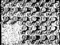 Figure 4b. Diamond Particles On Top Pads
Universal Tester Load Boards
Once an mBGA die has been seated in a carrier, it may be tested and burned-in as a conventional PGA part. Since the carrier presents a common footprint (20x20 PGA) for all die types, Sandia has designed universal load boards for our HP 82000 testers, and universal burn-in boards for Advanced MicroTechnology burn-in systems. Load boards are personalized for particular die types by jumpering the appropriate power and ground pins on the PGA socket to adjacent interstitial holes which connect to power and ground planes in the boards. These short (<0.1") jumpers provide low impedance connections suitable for at-speed tests over 100 MHz.
All die types shown in Table 1, except the SA3470 Microcontroller, have been thoroughly tested in mBGA carriers. These tests have included dc parameters, ac timing, and full functional vector sets performed over the voltage range 4.5V to 5.5V, and over the temperature range 0 ° C to 70 ° C. Over these ranges, mBGA carrier data has agreed very closely with corresponding test data from wire-bonded, commercially packaged parts. Table 3 shows typical maximum test frequency data.
TABLE 3. Fmax Test Data For mBGA and Commercial Packages
| Fmax at 0 ° C (MHZ) | Fmax at 70 ° C (MHZ) | ||||
| Dic Type | Package | 4.5 V | 5.5 V | 4.5 V | 5.5 V |
| MT5C2568 | mBGA | 72.5 | 80.6 | 67.6 | 75.7 |
| Commercial | 71.8 | 78.7 | 66.1 | 74.2 | |
| PDSP16515 | mBGA | 86.3 | 97.2 | 75.3 | 83.2 |
| Commercial | 88.0 | 98.9 | 77.3 | 85.0 | |
| LCA100106 | mBGA | 27.3 | 32.1 | 21.2 | 25.4 |
| Commercial | 25.6 | 30.8 | 20.0 | 24.1 | |
Universal Burn-in Boards
Sandia-designed burn-in boards for the AMT M300 system have 30 PGA sockets per board. One half of the sockets hold die carriers, referred to as DUTs (device under test). Each DUT position is connected to a socket which holds a PGA component carrier. Component carriers are unique to particular die types and contain passive components (jumpers, resistors, capacitors) which connect DUT pins to burn-in system signals.
Our burn-in studies are just beginning and data are limited to about 1000 hours each on eight carriers at 125 ° C and 5.5V. So far we have not observed any degradation or contamination of the die or carriers, except as noted earlier (elastomer interposers take a "set" and give erratic contact resistance, and particle interposers pit the solder bumps somewhat). The carriers, including particle interposers, appear to be robust under these burn-in conditions.
mBGA Attachment and Reliability Testing
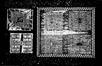 Figure 5. MCM-D Test Substrate With ATC03 And XC4010 mBGAs
Sandia has designed and is having fabricated a series of test substrates to evaluate mBGA attachment and rework processes, and the reliability of the attached die. Substrate materials include low temperature co-fired ceramic (MCM-C), polyimide/metal on alumina and silicon (MCM-D), and two types of FR-4 laminates (MCM-L). Each test substrate is about 1.3" square, contains one to four mBGAs, with die pads connected to a standard pattern of peripheral pads for electrical testing (Figure 5). Two types of mBGA test die are being used: 1) Sandia's Assembly Test Chips, ATC03 and ATC04, and 2) test die which have alternate pairs of peripheral pads shorted together so that a daisy chain of all bump connections can be formed with the substrate. The ATC die have heaters and various sensors for measuring moisture, corrosion, temperature, and strain. Two daisy chain die will be used. One, which emulates the peripheral pad layout of the Xilinx XC4010 FPGA, has 191 array pads on .030" pitch. The other emulates the peripheral pads of LSI Logic LCA 100106 ASIC and has 275 array pads on .020" pitch. The daisy chain mBGA die have been fabricated in both silicon and quartz. Clear quartz die give some visual access to the bump connections, which can augment X-ray inspection.
Using the test substrates, several mBGA attachment processes will be evaluated, including solders and conductive adhesives with and without underfill. Assembled substrates will be subjected to both mechanical and thermal shock, highly accelerated stress testing (HAST), and temperature cycling to determine the mechanical reliability of mBGA assemblies. Both environmental temperature cycling and power on/off cycling, using heaters on the ATC die, will be performed to obtain solder fatigue data.
Summary
Perhaps by the year 2000 area array die from IC suppliers will be common, but today they are scarce. mBGA technology offers a cost effective means for acquiring array die for flip-chip attachment today. Such die, with array pitches of .020" and .030". are easily placed in non-bonding die carriers for test and burn-in to assure a ''known good die" before assembly with commonly available placement equipment. Sandia has demonstrated mBGA fabrication and testing techniques, and has an internal program in progress to develop processes for attachment and rework, and to assess the reliability of MCM assemblies.
Acknowledgment The author wishes to thank many at Sandia who have provided funding. encouragement, and technical support for this work. Principal contributors have been R. L. Williams. P. V. Dressendorfer, and Rajen Chanchani. This work was performed at Sandia National Laboratories and Supported by the U. S. Department of Energy under contract DE-AC04-94AL85000.
References
Derman, Glenda, "Interconnects and Packaging," Electronic Engineering Times, Feb. 28, 1994, P. 61.
Vardaman, E. Jan et al, Worldwide Developments in Flip Chip Interconnect, TechSearch International, Inc., Feb. 1994, P. 22.
Particle Interconnect: A New Interconnect Technology
Larry DiFrancesco
Proceedings of the Surface Mount International Conference, MCM-L Interconnection Technology, August 1993
ABSTRACT
Fine Pitch surface mount technology is growing in acceptance. This market is also expanding in package variety. This increasing package shape variety results in more socket designs and toolings. Presently, developing a new socket requires significant tooling lead-time, resource commitment, and adequate projected production commitments. Included in this undertaking, is the acceptance of the new package in the electronics market.
To meet these difficulties, a fast response, low cost, easy to implement, alternate interconnect technology is needed. Particle Interconnect (PI) Technology appears to be just such a technology. PI is presently used in the electronics testing industry for creating very high performance, high frequency sockets and contactors. The PI socket has exceptional long life (+1,000,000 remates) and very high reliability. PI creates a remateable electrical interconnect on any electrical surface with the application of low mechanical force. This property allows a PI coated printed circuit board to be transformed into a high performance, high frequency, remateable socket.
INTRODUCTION
Advances in electronics have often focused on the dramatic improvements in the devices or processes associated with electronic manufacturing, (i.e., new chip architecture, printed circuit board material, surface mount technology and tape automated bonding technology.) Not to be overlooked, however, are the advancements and new applications being developed in interconnect technology and device socketting. In particular, the Z-axis connection systems are enjoying significant attention and are exploring the use of solderless, low-pressure electrical connections. These new technologies offer cost savings, and higher packing density.
The Z-Axis connection systems are being explored in an effort to improve time to market, reduce tooling costs, and improved performance. There are many Z-Axis technologies being examined. The various designs include: 1) carbon-filled ribs - either carbon fibers or particles, 2) silver-filled ribs or other metal powders, 3) metal-on-elastomer (MOE) - either metalized elastomer, 4) embedded fine wires, or 5) wrap-type designs consisting of a surface metallization, silicon skin or 6) flexible circuit wrapped over a silicone core, 7) stamped and formed contacts, 8) springwire contacts, and 9) fuzz buttons. Each of these approaches require a wiping action; high pressure concentration; and/or precious metal surfaces.
The contaminates and oxides present on metal contact surfaces mandate the wiping action to make reliable electrical connection. Even the metal-dot to metal-dot connections technology have a wiping action. The wiping action is due to the high compressive forces causing plastic deformation of the contact surface thus exposing the clean metal surface beneath. Work performed by different research groups indicates that the electrical connections are made through the asperities present on the ... electrical surface. The wiping action is a necessary requirement to bring the asperities into proximity. Equations were developed by one research consortium which indicate there is a relationship between contact-resistance, contact-force, the number of asperities, the size of the asperity, and the asperities distribution.
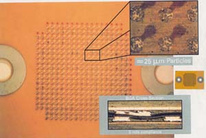
Consistent with this theory, Particle Interconnect (PI) technology forms a contacting surface that has a large number of "hertzian stress risers" or asperities (Figures 1 through 4). These asperities have very sharp and hard points due to the nature of the particle or crystal used (i.e., diamond, carbides, oxides, and other abrasive materials). The sharp points do not dull or wear since the crystal is much harder than the opposing metal surface. The conductive nature of the crystal is permanent and is enhanced due to support by the surrounding metal matrix. The size of the particle is carefully controlled with the notable absence of oversize particles. The particle's adhesion to the supporting surface is the most important feature of the PI process. A strong support or foundation must be present to prevent the particle from sinking in the supporting conductor when exposed to a high usage environment such as final production test performed by automatic test equipment (ATE) where millions of components must be tested.
Using a mature technology as an example, compare springwire contacts to standard stamp and formed contacts. The springwire contact has a number of independent springs that create multiple contact points along the pin-socket interface. This results in a large number of independent, parallel current paths. The parallel path provides higher contact reliability and durability with a large number of mating cycles; higher current capacity; lower contact resistance; and better performance in harsh dynamic environments.
The use of many parallel connections is a key feature in PI technology. The PI surface is like conductive sandpaper and like sandpaper has many points to penetrate any opposing surface. The PI surface is also similar to a micro-bed-of-nails. Like the bed-of-nails, the PI surface has many parallel paths for contact reliability and durability; a long cycle life; high current capacity; very low contact resistance; and PI forms a gas-tight joint for better performance in harsh dynamic environments.
A fact of nature states that: "to form an electrical connection between two surfaces, a mechanical requirement exists where at least one surface must be compliant". Hence, the need for springs to be present in all connection schemes. PI, when present between a compliant conductor and rigid surface, forms a low-resistance connection with very low force. The connection for this system is created when a pressure clamping device forces the sharp raised peaks into piercing contact with the mating surface. The PI joint is a pressure only connection which requires no sliding or wiping action. Thus the connection is not an element in the electrical chain, but is a matched impedance connection. With no impedance mismatch, there is no reflected energy. Reducing the amplitude of the reflected signal allows for faster signal transmission with greater signal fidelity.
A problem in high frequency testing and interconnects is the impedance mis-match between the device and related circuitry. This mismatch is typically caused by the use of conventional interconnect technology with its long, uncontrolled impedance environment. Due to physical characteristics, conventional interconnects force long trace lengths between devices and related circuitry. All of these factors contribute to increased resistance (R), capacitance (C), and inductance (L).
However, due to the superior physical characteristics of PI, and because PI contacts exhibit the same electrical characteristics as a solder connection, use of PI can effectively eliminate impedance mismatch experienced using conventional connection assemblies. The typical resistance of a conventional interconnect begins at approximately 30 milli-ohms with 100 grams of contact force and several mils of wiping travel for precious metal surfaces. The wiping action required by conventional interconnect technology destroys and scars the metal surface that is being wiped. The wiping surface accumulates the wiped-off debris, and its non-conductive materials. With time, this accumulated debris prevents any electrical connection from being formed.
The absence of wiping action and the low force required to make connection combine to simplify the requirements of the mechanical hold-down. Other connection schemes typically require 100 grams per contact. At 100 grams per contact, the force level for a 227 point land grid array (LGA) package socket would be approximately 50 pounds. The PI equivalent socket requires only 0.9 pound. High compressive force of conventional connections require the inclusion of a backing plate to stiffen the receiving surface. This stiffening plate is absent in the PI design.
EXPERIMENTAL DATA
Contact-resistance verses contact-force measurements were made on PI samples by outside testing labs. The tests confirm that only extremely low contact force is required to make a low contact resistance connection after 10 remates at the same contact-site. The test was performed using a hemispherical probe that was pressed against a plane of PI. To obtain accurate measurements of contact resistance, the hemispherical probe was one half of a 4-point probe system. The particlized plane was the other portion of the 4-point probe system. Since a hemisphere only makes contact to a plane at one point, this approach obtains the most accurate single point contact measurement data.
A computer controlled 4-point probe contact resistance test station was used to obtain the contact resistance verses contact force data (Figures 5 through 8). The probe made only vertical movements with no wiping action and contacted the same site multiple times (10 remates). The contact resistance measurement was made with a high accuracy 4-point probe digital meter. The contact force was monitored while the probe was pressed against the particlized surface.
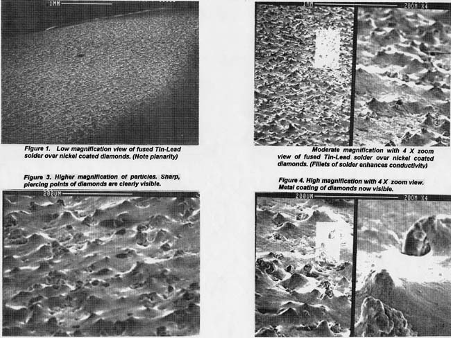
The test was made using a 250 mil diameter probe pressing against a planar copper foil surface covered with 20 to 25 micron diameter metalized particles. The particles were nickel coated with a fused tin-lead solder overcoat. The particles were attached to a 20 mil thick copper foil. A soft gold metal probe and a bright-tin metal probe were used in the experiments.
The bright-tin (BtSn) probe consisted of 125 micro-inch of bright-tin over 50 micro-inch of nickel.
The results of the contact resistance verses contact force test (Table 1) are:
| Probe type | Contact resistance | Contact force |
| gold probe | ~ 10 milli-ohms | 10 grams |
| bright tin (BtSn) probe | ~ 8 milli-ohms | 10 grams |
probe diameter = 0.250", max. current = 50 mA, max. voltage = 50 mV
TABLE 1. This table shows the contact resistance observed with minimum force available on the contact resistance/force test station for multiple test runs (10 remates) with a non-wiping spherical probe against a PI coated planar surface.
Changing the surface metal of the probe (gold or bright-tin against the tin/lead solder coated PI) did not change the resistance or force requirements. Conventional contacts would have had a significant performance difference between the two metal surfaces especially when remating at the same contact-site. Typically the gold surface is superior to the bright-tin surface, however, at a substantially increased cost.
It is important to observe the consistency of the PI coatings contact resistance verses the number of remates at the same point with no wiping action. The range of the reading at any given force is approximately 3 milli-ohms, which is superior for the industry. The four graphs (Figures 5 through 8) show the contact resistance consistency of the PI coated surface and the contact resistance inconsistency of the non-Pl coated surface. The inconsistent contact resistance of the non-PI surface is normal for the non-wiping connection. The values for the non-Pl coated surface depict an increasing resistance verses force during the 10 remates sequence of tests. This resistance increase is due to an oxide or contaminate building up on the contact-site. The non-PI coated resistance increase occurs because the contaminate is not swept away by contact wiping action.
Conventional contacts require 100 grams of contact force verses only 10 grams of contact force for PI. Because the contact force is so small for PI, other means for providing hold-down forces are open for consideration. These other hold-down methods include the use of adhesives, vacuum, and/or air pressure, besides low pressure springs and dips.
The purpose of these contact resistance verses contact force test is to quantify the properties of PI.
The use of the spherical probe against a PI coated plane isolates the resistance verses force parameters from other issues such as contact resistance verses current carrying capacity. To observe contact resistance verses current carrying capacity, a 10 mil wide pad on a compliant surface (flex-circuit) was damped against a broad sheet of copper foil. A 4-point probe resistance measuring system was established with one set of the probe wires soldered to the pad-under-test. The other set of probe wires were soldered to the sheet of copper. A light damping force of 10-20 grams was applied. The voltage drop across the contact was monitored while the forcing current was increased (Table 2).
Contact resistance vs current capacity
| Forcing current Amps |
Sense voltage milli-volts |
Resistance (R = V / I) milli-ohms |
| 0.0001 | too small to read | - |
| 0.0010 | too small to read | - |
| 0.0100 | 0.0113 | 1.13 |
| 0.1000 | 0.1243 | 1.24 |
| 0.2000 | 0.2480 | 1.24 |
| 0.3000 | 0.3751 | 1.25 |
| 0.4000 | 0.5011 | 1.25 |
| 0.5000 | 0.6351 | 1.27 |
| 0.6000 | 0.7660 | 1.27 |
| 0.7000 | 0.9042 | 1.29 |
| 0.8000 | 1.0240 | 1.28 |
| 0.9000 | 1.1631 | 1.29 |
| 1.0000 | 1.2796 | 1.28 |
| 1.5000 | 1.8978 | 1.26 |
| 2.0000 | 2.5438 | 1.27 |
Table 2. This chart shows the current capacity verses contact resistance of a 10 mil wide pad held against a broad copper plane with 10 - 20 grams of clamping force.
PI technology has been used in the electronic testing industry for creating very high performance sockets and contactors. The PI contactor has exceptional longlife. A PI coated printed circuit board creates a socket on any electrical surface when a light contact force is applied. This property allows a printed circuit board to be transformed into a high performance socket.
EXAMPLES OF APPLICATION
PI has been used in many high frequency, high performance, longlife applications. In particular, contactors for automatic test equipment (ATE) and handlers. The contactor, normally is a standard bent-wire socket with the lid removed if used in a handler. The normal bent-wire contactor is limited to accept only one style package per contactor design. A high cost is incurred if many different pin count package/contactors must be stocked. Since handlers are longlife only a few contactors are required which results in a high cost per contactor due to tooling cost.
A PI contactor consists a coating of PI on a print circuit board. This simplicity of construction allows for flexibility in designing contactors with the shortest lead length possible. Also, multiple package styles can be nested in one design. An example of nesting multiple packages can be seen in Figure 9. Six different pin count packages can be accommodated by this contactor. All packages were 20 mil pitch, quad flat packs (QFPs). The particles were on both sides of the flex circuit and allowed high speed testing of each package style without changing the tester interface board. The result was a significant cost savings and increased product throughput. The packages under test were developmental and the customer saved considerable time-to-market by using the fast response time of designing with PI. The customer avoided high tooling cost, or the purchase of many dedicated tester interface boards.
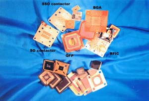
Figure 10 is a family of PI interposers fabricated on flex-circuit for high frequency use or developmental package evaluations. The upper-right object is a ball grid array (BGA) package PI interposer. The BGA is a 15 X 15 pad (225) array on 50 mil pitch. The pads were relocated to a convenient 100 mil pitch, through-hole, pin grid array (PGA), pin-out. The lower-right object is a 256 pin, 20 mil pitch, QFP interposer. This PI interposer allows the testing, characterizing, burn-in, and remating of a 20 mil pitch, formed lead package. This feature was important since the device under test was a gallium-arsenide ASIC with a clock-speed greater than 500 MHz. The PI interposer allowed the device to be evaluated in the same configuration as when the device is soldered to the application board. This allowed a 6 to 18 month time-to-market improvement because a more accurate characterization of the device was performed. The lower-left PI interposer is a 40 pin, 50 mil pitch, 150 mil wide body, universal SO contactor. This is a nested design for many of the 150 mil wide body SO packages. The upper-left PI interposer is a 40 pin, 20 mil pitch, universal SSO contactor. This is a nested design for many of the SSO packages.
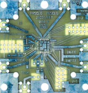
Figure 11 is a rigid circuit, 12 GHz test board for testing radio frequency IC (RFICs). The test board was designed for controlled impedance connections to the device under test (DUT), with control logic signals and terminations in close proximity. Components are mounted on both-sides of this test board. Production devices are characterized under ideal signal measurement conditions. Higher device yields are realized because smaller, more realistic guard-bands can be set and testing can be performed at near operating conditions.
Figure 12 shows the use of PI on flex-circuit material to form a translator bare-board test fixture. The translator is constructed by using a simple two-sided, plated-through-hole, printed circuit board (PCB), which is coated with PI on both-sides. The translator PCB uses the printed circuit board to accommodate the difference between off-grid test points of the unit under test (UUT) and the universal grid of the board test system. The bottom side matches up with the testers on-grid pads. Traces from the bottom side connect to the top side with plated-through holes. The translators PCB becomes the test fixture. The particles of the PI leave a small and characteristic impression on the UUT test points. This board has been tested over 10 times (Figure 13). The size of the probe point in this fixture was set at 16 mils in diameter to engage the 20 mil pad pitch on the UUT. Other pad pitches are available by defining the PI pad artwork. This UUT had over 2,000+ test points. The 2,000+ test points, typically, measured under 10 milli-Ohms after being exercise at least 10 times.
FUTURE INITIATIVES
The PI technology is in its early development stages, but initial customer feedback and field reports would indicate these efforts are focused in the right direction! As previously mentioned, the need for more design applications is evident, and research into other areas of use have been initiated. Result updates are anticipated within the next 12 months.
CONCLUSION
PI creates a non-wiping, remateable interconnect with properties required for very high performance, high frequency, long-life contactor, socket, or interconnection. PI is easy to implement, offers quick turn-around, and minimum tooling or design effort. A PI coated printed circuit board creates a socket on any electrical surface when a light contact force is applied.
ACKNOWLEDGEMENTS
The author would like to thank the following individuals for their engineering assistance and input to this article:
- Steven D. Clark, Northrop Corp, Orange, California
- Kong Xiong, ACSIST Associates lnc, Minneapolis, Minnesota
- Victor Morse, Exatron A.T.E., San Jose, California
References
L. DiFrancesco and C. Reynolds, ACSIST Associates Inc. "Socketing Chip-On-Board to a Multichip Module Using Particle Interconnect," 1993 International Conference and Exhibition on Multichip Modules, ISHM/IEPS 531-VC, April 1993.
L. DiFrancesco, "Method for Cold Bonding," U.S. Patent 4,804,132 (14 Feb 1989).
L. DiFrancesco, "Particle-Enhanced Joining of Metal Surfaces," U.S. Patent 5,083,697 (28 Jan 1992).
H. W. Markstein,"MCM-L Offers Easiest Path to Higher Performance," Electronic Packaging & Production (Jan 1993).
B. Grove, "Z-Axis Adhesive Film," Interconnect Technology, (Dec 1992).
S. J. Roberts and T. Shepler, "Flexible Circuit Substrates," Interconnect Technology, (Dec 1992).
R. H. Eberlein, "High-Reliability Springwire Contacts for Critical Applications," Connection Technology, (Jan 1991).
D. Bonnette and D. Murphy, "A Flexible Circuit Controlled Impedence Interconnect System," Connection Technology, (June 1990).
Biography:
Mr. Larry DiFrancesco has over 17 years work experience in the Advanced Packaging Research and Development. He is Presently responsible for installing the Particle Interconnect Process at ACSIST Associates Inc. which recently purchased the exclusive patent rights from Exatron. At Exatron, Mr. DiFrancesco was PI Product Manager, where he developed the initial process and created many of the present designs and applications. Prior to working for Exatron, Mr. DiFrancesco was a project leader on an advanced MCM-D Flip-Chip packaging program at Hughes Aircraft Co. and other R&D packaging projects for over 10 years.
Mr. DiFrancesco has presented and published several papers related to Advanced Packaging and Fine Pitch Surface Mount Technology. Mr. DiFrancesco presently has three patents in the Advanced Packing field. He received his BS in Electronics Engineering from CalPoly, San Luis Obispo Cal. in 1976.
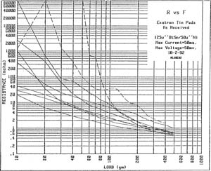
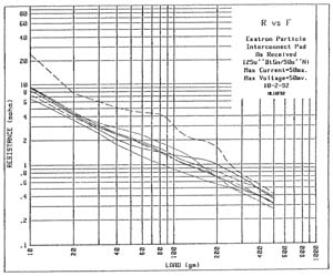
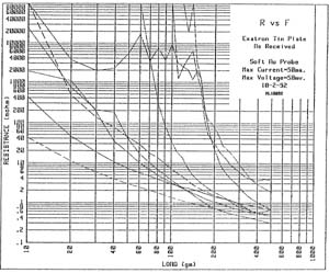
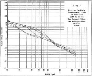
Contact resistance (milli-Ohm) vs. holddown force (gram-force)
0.25" diameter hemispherical probes vs. 63/37 tin-lead coated surface.
| Figure 5: Bright tin probe vs. control (no PI) | Figure 7: Bright tin probe vs. 20-25 μ PI |
 |
 |
|
. 0.010" BeCu, 0.250" Ni, 0.150" SnPb. . 20 to 80,000+ milli-Ohms, 1 to 9 remates. . No scrubbing action. |
. 0.010" BeCu, 0.250" Ni + PI, 0.150" SnPb. . 6 to 9 milli-Ohms (one ignored), 1 to 6 remates. . No scrubbing action against PI. |
| Figure 6: Gold Probe vs. Control (no PI) | Figure 8: Gold probe vs. 20-25 μ PI |
 |
 |
|
. 0.010" BeCu; 0.250" Ni; 0.150" SnPb. . 20 to 80,000+ milli-Ohms, 1 to 9 remates. . No scrubing action. |
. 0.010" BeCu; 0.250" Ni + PI; 0.150" SnPb. . 8 to 14 milli-Ohms, 1 to 8 remates. . No scrubbing action against PI. |
 |
 |
| Figure 9: A Nested PI contactor with 6 different pin count, 20 mil pitch QFP packages. | Figure 10: A family of PI interposers, 225 pad BGA contactor, 256 pin 20 mil pitch QFP contactor, 40 pin 50 mil pitch Universal SO package contactor, 40 pin 20 mil pitch Universal SSO package contactor. |
 |
|
| Figure 11: A rigid circuit 12 Ghz test board for testing radio frequency IC with terminations in close proximity. | Figure 12: A translator bare-board test fixture using PI on both sides for probing fine pitch PCBs. |
Picture not shown.
Figure 13: A 20 mil pad pitch PCB after being tested at least 10 times with a PI translator bare-board test fixture.
Socketing Chip-On-Board to a Multichip Module Using Particle Interconnect
Larry DiFrancesco, and Carl Reynolds
1993 International Conference and Exhibition on Multichip Modules, ISHM/IEPS 531-VC, April 1993.
Abstract
It is proposed that a recently developed technology, Particle Interconnect, may be used to create a socket, form a remateable interconnect, or possibly form an attachment for a Chip-On-Board (COB) applications in a multichip module (MCM-L).
Presently Particle Interconnect (PI) technology is used in the electronics testing industry for creating very high performance, high frequency sockets and contactors. The PI socket has exceptional longlife (+1,000,000 remates) and reliability. PI creates a remateable electrical interconnect on any electrical surface with the application of low mechanical force. This property allows a printed circuit board to be transformed into a high performance, high frequency, remateable socket.
While standard COB technology is acknowledged to be the lowest cost packaging technology available. COB technology's main disadvantage is the lack of device testability. By combining standard COB technology with the PI coating, the disadvantages of standard COB technologies are eliminated. This improved COB mounted device has an integrated socket. PI thus allows for COB testing, burn-in, programming, and mounting to the MCM circuit board with the same confidence as standard coarse pitch packaged devices.
KEYWORDS: Particle, Interconnection, Known good die, Packaging, MCM-L
Advances in electronics have often focused on the dramatic improvements in the devices or processes associated with electronic manufacturing. (i.e., new chip architecture, printed circuit board material, surface mount technology and tape automated bonding technology.) Not to be overlooked, however, are the advancements and new applications being developed in interconnect technology. In particular the Z-Axis connection systems are enjoying significant attention. As the electronics industry increases demand for high I/O count devices and packages, many programs are exploring the use of solderless, low-pressure electrical connections.
The limitations of present technology do not allow the device (or chip) to be placed in a socket environment such as testing, burn-in, or programming prior to attachment. Standard Chip-On-Board (COB) is currently acknowledged to be the lowest cost packaging technology. The main disadvantage for COB technology is the lack of device socket-ability. To address this shortcoming, the Z-Axis connection systems are being explored. There are many approaches to the problem. The various designs include: 1) carbon-filled ribs - either carbon fibers or particles, 2) silver-filled ribs or other metal powders, 3) metal-on-elastomer (MOE) - either metalized elastomer, 4) embedded fine wires, or 5) wrap-type designs consisting of a surface metallization, silicon skin or 6) flexible circuit wrapped over a silicone core, 7) stamped and formed contacts, 8) springwire contacts, and 9) fuzz buttons. Each of these approaches requires a wiping action; high pressure concentration; and/or precious metal surfaces.
The contaminates and oxides present on metal contact surfaces mandate the wiping action to make reliable electrical connection. Even the metal-dot to metal-dot connections technology have a wiping action. The wiping action is due to the high compressive forces causing plastic deformation of the contact surface thus exposing the clean metal surface beneath. Work performed by different research groups indicates that the electrical connections are made through the asperities present on the surface. The wiping action is a necessary requirement to bring the asperities into proximity. Equations were developed by one research consortium which indicate there is a relationship between contact-resistance, contact-force, the number of asperities, the size of the asperity, and the asperities distribution.
Consistent with this theory. Particle Interconnect (PI) technology forms a contacting surface that has a large number of hertzian stress risers or asperities (Figures 1 through 4). These asperities have very sharp and hard points due to the nature of the particle or crystal used (i.e., diamond, carbides, oxides, and other abrasive materials). The sharp points do not dull or wear since the crystal is much harder than the opposing metal surface. The conductive nature of the crystal is permanent and is enhanced due to support by the surrounding metal matrix. The size of the particle is carefully controlled with the notable absence of oversize particles. The particle's adhesion to the supporting surface is the most important feature of the PI process. A strong support or foundation must be present to prevent the particle from sinking in the supporting conductor when exposed to a high usage environment such as final production test performed by automatic test equipment (ATE) where millions of components must be tested.
Using a mature technology as an example, compare springwire contacts to standard stamp and formed contacts. The springwire contact has a number of independent springs that create multiple contact points along the pin-socket interface. This results in a large number of independent, parallel current paths. The parallel path provides higher contact reliability and durability with a large number of mating cycles; higher current capacity; lower contact resistance; and better performance in harsh dynamic environments.
The use of many parallel connections is a key feature in PI technology. The PI surface is like conductive sandpaper and like sandpaper has many points to penetrate any opposing surface. The PI surface is also similar to a micro-bed-of-nails. Like the bed-of-nails, the PI surface has many parallel paths for contact reliability and durability; a long cycle life; high current capacity; very low contact resistance; and forms a gas-tight joint for better performance in harsh dynamic environments.
A fact of nature states that: "to form an electrical connection between two surfaces, a mechanical requirement exists where at least one surface must be compliant". Hence, the need for springs to be present in all connection schemes. PI, when present between a compliant conductor and rigid surface, forms a low-resistance connection with very low force. The connection for this system is created when a pressure clamping device forces the sharp raised peaks into piercing contact with the mating surface. The PI joint is a pressure only connection no sliding or wiping action is required. Thus the connection is not an element in the electrical chain, but is a matched impedance connection and does not cause an impedance mismatch. With no impedance mismatch there is no reflected energy. Reducing the amplitude of the reflected signal allows for faster signal transmission with greater signal fidelity.
A problem in high frequency testing and interconnects is the impedance mis-match between the device and related circuitry. This mismatch is typically caused by the use of conventional interconnect technology with its long, uncontrolled impedance environment. Due to physical characteristics, conventional interconnects force long trace lengths between devices and related circuitry. All of these factors contribute to increased resistance (R), capacitance (C), and inductance (L).
However, due to the superior physical characteristics of PI, and because PI contacts exhibit the same electrical characteristics as a solder connection, use of PI can effectively eliminate impedance mismatch experienced using conventional connection assemblies. The typical resistance of a conventional interconnect begins at approximately 30 milli-ohms with 100 grams of contact force and several mils of wiping travel for precious metal surfaces. The wiping action required by conventional interconnect technology destroys and scars the metal surface that is being wiped. The wiping surface accumulates the wiped-off debris and its non-conductive materials. With time this accumulated debris prevents any electrical connection from being formed.
The absence of wiping action and the low force required to make connection combine to simplify the requirements of the mechanical hold-down. Other connection schemes typically require 100 grams per contact. At 100 grams per contact, the force level for a 227 point land grid array (LGA) package socket would be approximately 50 pounds. The PI equivalent socket requires only 0.9 pound. High compressive force requires the inclusion of a backing plate to stiffen the receiving surface. This stiffening plate is absent in the PI design.
Contact-resistance verses contact-force measurements were made on PI samples by outside test labs. The tests confirm that extremely low contact force is required to make a low contact resistance connection. The test was performed using a spherical probe that was pressed against a plane of PI. To obtain accurate measurements of contact resistance, the spherical probe was one half of a 4-point probe system. The particlized plane was the other portion of the 4-point probe system. Since a sphere only makes contact to a plane at one point, this approach obtains the most accurate single point contact measurement data.
A computer controlled 4-point probe contact resistance test station was used to obtain the contact resistance verses contact force data (Figures 5 through 8). The probe made only vertical movements with no wiping action and contacted the same site multiple times. The contact resistance measurement was made with a high accuracy 4-point probe digital meter. The contact force was monitored while the probe was pressed against the particlized surface.
The test was made using a 250 mil diameter probe pressing against a planar copper foil surface covered with 20 to 25 micron diameter metalized particles. The particles were nickel coated with a fused tin-lead solder overcoat. The particles were attached to a 20 mil thick copper foil. A soft gold metal probe and a bright tin metal probe were used in the experiments. The bright-tin (BtSn) probe consisted of 125 micro-inch of bright-tin over 50 micro-inch of nickel. The results of the contact resistance verses contact force test (Table 1) are:
| Probe type | Contact resistance | Contact force |
| gold probe | ~ 10 milli-ohms | 10 grams |
| bright tin (BtSn) probe | ~ 8 milli-ohms | 10 grams |
TABLE 1. This table shows the contact resistance observed with minimum force available on the contact resistance/force test station for multiple test runs with a non-wiping spherical probe against a PI coated planar surface.
Changing the surface metal of the probe (gold or bright-tin against the tin/lead solder coated PI) did not change the resistance or force requirements. Conventional contacts would have had a significant performance difference between the two metal surfaces. Typically the gold surface is superior to the bright-tin surface, however at a substantially increased cost.
It is important to observe the consistency of the PI coatings contact resistance verses the number of remates at the same point with no wiping action. The range of the reading at any given force is approximately 3 milli-ohms, which is superior for the industry. The four graphs (Table 2) show the consistency of the PI coated surface and the inconsistency of the non-PI coated surface. The inconsistency of the non-PI surface is the norm for the non-wiping connection. The values for the non-PI coated surface depict an increasing resistance verses force sequence of tests. This resistance increase is due to an oxide or contaminate increase on the surface. This increase occurs because the contaminate is not swept away.
Conventional contacts require 100 grams of contact force verses only 10 grams of contact force for PI. Because the contact force is so small other means for providing hold-down forces are now open for consideration. These other hold-down methods include the use of adhesives, vacuum, and/or air pressure.
The purpose of these contact resistance verses contact force test is to quantify the properties of PI. The use of the spherical probe against a PI coated plane isolates the resistance verses force parameters from other issues such as contact resistance verses current carrying capacity. To observe contact resistance verses current carrying capacity a 10 mil wide pad on a compliant surface (flex-circuit) was clamped against a board sheet of copper foil. A 4-point probe resistance measuring system was established with one set of the probe wires solder to the pad-under-test. The other set of probe wires were solder to the sheet of copper. A light clamping force of 10-20 grams was applied. The voltage drop across the contact was monitored while the forcing current was increased.
| Forcing current Amps |
Sense voltage milli-volts |
Resistance (R = V / I) milli-ohms |
| 0.0001 | too small to read | - |
| 0.0010 | too small to read | - |
| 0.0100 | 0.0113 | 1.13 |
| 0.1000 | 0.1243 | 1.24 |
| 0.2000 | 0.2480 | 1.24 |
| 0.3000 | 0.3751 | 1.25 |
| 0.4000 | 0.5011 | 1.25 |
| 0.5000 | 0.6351 | 1.27 |
| 0.6000 | 0.7660 | 1.27 |
| 0.7000 | 0.9042 | 1.29 |
| 0.8000 | 1.0240 | 1.28 |
| 0.9000 | 1.1631 | 1.29 |
| 1.0000 | 1.2796 | 1.28 |
| 1.5000 | 1.8978 | 1.26 |
| 2.0000 | 2.5438 | 1.27 |
Table 2. This chart shows the current capacity verses contact resistance of a 10 mil wide pad held against a broad copper plane with 10 - 20 grams of clamping force.
Particle Interconnect technology has been used in the electronic industry for creating very high performance sockets and contactors. The PI contactor has exceptional longlife. PI creates a socket on any electrical surface when a light contact force is applied. This property allows a printed circuit board to be transformed into a high performance socket. The PI technology is a scalable process and can be reduced in pitch and pad dimension. The present work has been done with a Chip-On-Board application. The laminate material was pattemed both sides to form a chip carrier. The chip side of the chip carrier had a chip mounted and wire bonded to its surface. The wire bond pad was connected to the PI coated pad on the downside of the chip carrier by a plated through via. PI particles coated the downside of the chip carrier pad. The PI coated pad created the interconnect surface to the substrate pad site.
Once the chip was attached and wire bonded to the chip carrier, it is a packaged device. This packaged device can be socketed for operations such as testing, burn-in, and programming. The chip carrier protects the chip from damage and allows easier handling. The chip carrier spreads the fine pitch of the chip to the coarse pitch of the socket. The test site uses vacuum or mechanical clamping to hold the chip carrier to the coarse pitch of the test site.
PI has been very successful at making contact to a conducting surface with both coarse particles and fine particles. The coarse particles are for coarse geometry's while the fine particles are for fine geometry's. Preliminary work with fine particles has demonstrated the ability to make connection to bumped chips. It is speculated that PI coated surfaces can be used for Direct Chip Attach (DCA) or for probing chips using a membrane probe card. Using a PI surface as means to interconnect a chip for probing and screening, it is possible to identify Known Good Die (KGD).
Since PI creates a non-wiping, remateable interconnect with the properties required for very high speed performance, testing chips at-speed is becoming a reality. It is envisioned that PI can be used for array bumped C4 die interconnect without the requirements for advanced handling technologies. Acsist will be starting a program to explore the use of PI in this advanced packaging arena.
REFERENCES
L. DiFrancesco, "Method for Cold Bonding," U.S. Patent 4,804,132 (14 Feb1989).
L. DiFrancesco, "Particle-Enhanced Joining of Metal Surfaces," U.S. Patent 5,083,697 (28 JAN 1992).
H. W. Markstein, "MCM-L Offers Easiest Path to Higher Performance," Electronic Packaging & Production (JAN 1993).
B. Grove. "Z-Axis Adhesive Film," Interconnection Technology, (DEC 1992)
S. J. Roberts and T. Shepler, "Flexible Circuit Substrates," Interconnection Technology (DEC 1992).
R. H. Eberlein, "High-Reliability Springwire Contacts for Critical Applications," Connection Technology (JAN 1991).
D. Bonnette and D. Murphy, "A Flexible Circuit Controlled Impedance Interconnect System," Connection Technology, (JUN 1990).
Contact resistance (milli-Ohm) vs. holddown force (gram-force)
0.25" diameter hemispherical probes vs. 63/37 tin-lead coated surface.
| Figure 5: Bright tin probe vs. control (no PI) | Figure 7: Bright tin probe vs. 20-25 μ PI |
|
|
|
. 0.010" BeCu, 0.250" Ni, 0.150" SnPb. . 20 to 80,000+ milli-Ohms, 1 to 9 remates. . No scrubbing action. |
. 0.010" BeCu, 0.250" Ni + PI, 0.150" SnPb. . 6 to 9 milli-Ohms (one ignored), 1 to 6 remates. . No scrubbing action against PI. |
| Figure 6: Gold Probe vs. Control (no PI) | Figure 8: Gold probe vs. 20-25 μ PI |
|
|
|
. 0.010" BeCu; 0.250" Ni; 0.150" SnPb. . 20 to 80,000+ milli-Ohms, 1 to 9 remates. . No scrubing action. |
. 0.010" BeCu; 0.250" Ni + PI; 0.150" SnPb. . 8 to 14 milli-Ohms, 1 to 8 remates. . No scrubbing action against PI. |
Particle Interconnect (PI) Technology, What Can It Do For You
Carl V. Reynolds
Abstract
Globally, the electronics industry is entering a new revolutionary era where improvements in performance, size, shape, weight and useful life are being demanded in unprecedented ways. This packaging and interconnection revolution in form factor is being driven by a combination of increasing functionality per unit area of silicon and the convergence of communications and computing products epitomised by the new generations of nomadic electronics products, such as wireless PDAs, notebooks, cellular phones in notebook computers etc. The resultant increase in packaging density is being driven to the base packaging level i.e. the interconnect substrate; and to the need to be able to test both packaged and unpackaged integrated circuits with test socket or probe connections which closely emulate the same connection which the device will have when connected to the product it is destined for. Today these high performance and density packaging and interconnection substrates are generically referred to by such names as, MCM-C, D, L or combinations of same depending on whether they are made from ceramic, deposited materials such copper or polyimide or laminate. The input/output pitch of the integrated circuit are common regardless of base interconnect substrate used. These pitches are usually specified in micro meters or mils, and may range from 100 um or 4 mils up to 20 mils. Therefore there is a great need for a test solution for these high density interconnect substrates. Similarly there is a need for a test solution for the high performance packaged or unpackaged integrated circuits which will be attached to these substrates, using test and or production sockets which enable at speed testing without minimum degradation of the test environment. These two are often referred to by users as Known Good Substrates (KGS) and Known Good Die or Devices (KGD). This test problem touches all facets of this new nomadic computing and communications world and ACSIST is exploring a number of different approaches to establish a reliable and cost effective solution for both its own and its customers use and benefit. Particle Interconnect (PI) is one of these approaches and it is being used successfully in a number of applications. This paper will outline what PI is, some current applications and evolving developments which maybe of help in your developments, as always , you the informed beholder must decide if it or an alternative solution is in your future.
Introduction
Particle Interconnect (PI)* is a patented means of forming separable or permanent connections between surfaces, with no wiping action as generally found and used ... The contacting surfaces are formed by the inclusion of a hard surface with many separate electrically conductive sharp points which when "Z' axis pressure is applied will penetrate the surface oxides on the parts to be connected. Thus with relatively low applied forces a permanent or separable electrical connection maybe formed which has the following characteristics. Low resistance per unit area, low inductance, low normal forces combined with a very small footprint. These low profile and area electrical contacts maybe incorporated into many different rigid and flexible structures; and by the application of well thought out designs can embody a certain amount of "Z" axis compliance.
DEVICE TEST CURRENT APPLICATIONS
Today the most prevalent insertion of this technology is into test handlers for packaged integrated circuits. In some high volume applications, even though some integrated circuit packages have integral compliance, such as gull wing or J-leaded devices some do not for example ceramic leadless packages, it is preferable to incorporate some degree of compliance in the test handler socket. This is done by incorporating a diving board type structure into which PI is incorporated.
Companies developing and supplying high performance Radio Frequency (RF) integrated circuits face a particularly difficult set of challenges in attempting to characterise these and emulate the packaged devices usage environment. This problem is resolved by eliminating the test socket which normally sits on top of the DUT board and incorporating PI directly into the DUT board or inserting a low profile PI based interposer between the device and the DUT board.
Ball Grid Arrays (BGAs) represent a new generation of low profile and cost packages which are expected to become pervasive in electronics packaging and interconnection. For several reasons these devices represent a new test challenge and the current flow is to assemble and package die to the BGA substrate and then route it through test and burn in. Following test and burn in the solder balls are attached to the base of the BGA package. This is recognised by the industry as a suboptimum solution and work is under way to improve on this. Using current spring based materials to make sockets is useful for integrated circuits packaged in BGAs up to a certain speed, however emerging generations of microprocessors and their attendant families of ASICS and memories cannot be adequately characterised and tested at full speed using this conventional approach. This application is a natural for applying PI and enables the design and manufacture of burn in boards with higher device counts per burn in board and oven load than conventional test socket solutions. These devices may also be tested out at full speed either on the normal DUT arrangement or with many mounted on a burn in board.
The rapid growth in programmable devices demands a test environment which requires a programming socket which makes consistent and reliable contacts. Industry data indicates that a considerable number of good devices are rejected and or damaged by the repeated insertion and removal which devices undergo into and out of conventional spring based sockets which need to have a clear wiping action to make a good electrical contact. The use of PI based sockets for programming of these devices has improved overall yields in these types of applications. This has come from the elimination of, miss-contacts and lead damage to the devices under test.
LEADING EDGE DEVICE TEST DEVELOPMENT
Whilst testing and burning in packaged devices is becoming increasingly more challenging, the next big challenge is to find a reliable and cost effective means of testing and burning in unpackaged integrated circuits and later whole wafer test and burn in. PI is in the early stages of these applications. The first successful application on unpackaged integrated circuits (IC) is on a solder bumped device. This is accomplished by the application of a minaturised interposer i.e. a scaled down version of the structure used on testing and burning in BGAs. This particular application will evolve so that both unpackaged and minimally packaged devices such as micro ball grid arrays, on area arrays with 10 mil pitches or less maybe tested and burned in with this or other evolutionary solutions.
SUBSTRATE TEST APPLICATION DEVELOPMENT
All types of MCM substrates have a several common manufacturing and test applications. One of the most challenging [problems] the industry faces is a reliable and cost effective solution for testing the high density features during ... process[ing] and at final substrate ... [test]. This high density test requirement is also becoming a requirement for dense printed circuit boards which use high density TAB or TAB like surface mount gull wing packages. It is also expected that future generations of BGAs or micro ball grid arrays on area array pitches of 20 mils and less, when used in large quantities on these dense printed circuit boards will also require breakthroughs in test probing technology.
A key driving factor is that whilst most bed of nails testers may have sufficient pin contact points available on an overall basis there may well be a shortage on a local basis; since the input/output area contact density will be greater than that available from the standard hundred mil grid of pogo pins.
The application of PI and other high density probing technologies is being explored as a possible solution. This requires several new developments in the probing structure, however what is common and attractive in all approaches is that the retention of the ability to use the large installed base of bed of' nails testers is possible except for the densest of substrates.
Controlled impedance to lead of package
 |
 |
| Schematic for controlled impedance socket. | Surface of PLCC J-Lead after 30,000 insertions. Surface finish of lead passed steam aging test. |
Controlled impedance socket
44 pin controlled impedance Particle Interconnect PLCC socket or interposer with singulate leads. Decoupling capacitors are within 0.100" of PLCC pad.
 |
 |
| Printed circuit board layout | Mechanical hold down |
Circuit layout for controlled impedance socket
D.U.T. board layout use for TDR measurement. The traces are narrowed to compensate for Z0 change due to devices present in the socket.
 |
 |
TDR of controlled impedance Particle Interconnect socket (interposer) on load board
 |
 |
||||||||||||||||||||||||||||||
|
|
||||||||||||||||||||||||||||||
|
|||||||||||||||||||||||||||||||
- Cursor at contact point on diamond dust/diving board with no part in socket.
- Trigger is continuously running at 10.0 kHz with step on.
- Demonstrated controlled impedance connector from contactor board to mother board using Particle Interconnect with impedance tolerance of 50 Ω ± 1 Ω.
- Controlled impedance of J-lead going to package.
- Compensation (Point 2 on graph) to neutralize internal inductance and capacitance of PLCC package (Point 3 on graph).
- Particle Interconnect is 10 times better than SMA connector (Point 1 on graph).
- Additional work by MMS, TI, and HP.
Process cost comparison
8 pin DIP vs. Particle Interconnect flip chip or smart card package
Particle Interconnect package description:
- Part size 0.47" x 0.43" suitable for flip chip or smart card part
- Dielectric - polyester @$6.00/pound = $0.000089/part
- @ 0.002" thick x 12" wide x 1154.4" long = 67,100 parts/pound
- @ 0.006" thick x 12" wide x 384.8" long = 22,350 parts/pound
- Particle Interconnect trace and via figured at $0.25/ft2 = $0.0103/part
| 0.100" pitch 8 pin Dual Inline Package | 0.004" - 0.100" pitch flip chip through 4 pin smart card | |
| Lead frame material | $0.015 | $0.0103 |
| Plastic material | $0.015 | $0.000089 |
| Wire for bonding | $0.005 | $0.00 |
| Labor | $0.015 | $0.015 or less |
| Overhead | $0.030 | $0.030 or less |
Particle Interconnect - Cray J90 repackaging
Particle Interconnect, enabled the repackaging of the Cray J90 Vector Processor, by increasing connector density by about 100 times while maintaining ultrahigh speed signal integrity.
Reducing Cray form factor using PI
Particle Interconnect - ACI
A Novel Interconnect Technology
Mark Allemang
empfasis November 2006
Electrically Transparent Connector
Moving Toward the Transparent Connector
By Dr. Eric Bogatin
...
The shorter an interface is compared to about 1/10th a wavelength of the highest frequency component, the more transparent it looks. For example, in a polymer dielectric, 1/10th of a wavelength at 10 GHz is about 1.5 mm or 60 mils. At 40 GHz, less than 0.4 mm or 15 mils is short.
...
A second technology solution for approaching a transparent connector is offered by Particle Interconnect Research and Development Inc. (http://www.pitek.us). Diamond dust particles are occluded in nickel plating and then overplated with gold. The plating can be applied to circuit board pads, flex pads, and even contactor points.
...