Removable Interconnect
Properties
Diamond Particle Interconnect interposer vs. solder ball

TDR data illustrates zero reactance and remate consistency of Diamond Particle Interconnect socket. TDR data shows that Diamond Particle Interconnect remated connection is better than soldered connection and SMA connector. Solder balls degradation shown in the inset. While Diamond Particle Interconnect is consistent across remates. State of the art Kyocera BGA package has very large impedance discontinuity.
10 Gb/s PAM4 (Programmable Attribute Map) eye diagram

6.25 Gb/s NRZ, PRBS (Pseudo Random Bit Sequence) 231-1 eye diagram

Particle Interconnect BGA interposer test setup
Nominal losses stem from the typical minimum interconnect surface area for BGA and other MLF type packages. However, the Particle Interconnect interposer minimizes these skin effect losses by maximizing surface area of the conductor (similar to multi-strand wire vs. single strand wire of same cross-section), thereby reducing transmission loss across the connection.
 |
 |
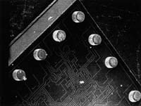
| Board | Testing of Particle Interconnect interposer for 676 ball BGA. |
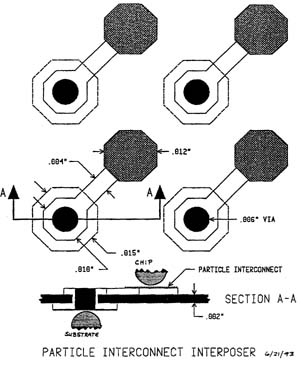
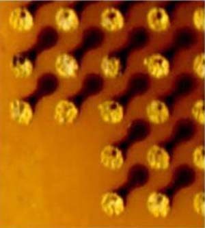
Particle Interconnect BGA interposer geometry
 |
 |
| 1 layer deflected PI interposer cross-section | 2 layer PI interposer |
 |
 |
| 2 layer deflected PI interposer | 2 layer deflected PI interposer cross-section |
Particle Interconnect vs. pogo pin S11 parameters
The measured insertion and return loss shows a 4 GHz resonance at the solder ball causing PCI-X return loss failure below 6 GHZ. By replacing the standard pogo pin socket with Particle Interconnect socket the return and insertion was measured beyond 12 GHz, without modifying the board.

Particle Interconnect contact resistance vs. contact force

Gold probe to top side Particle Interconnect
Particle Interconnect's very low resistance results in higher current capacity.
- 1 mm pitch BGA interposer.
- 9.2 grams contact force (.0902 N, .020 lbs, or .325 Oz.), 12 amps.
- Contact resistance = .00433 Ω
 |
 |
| Particle Interconnect array top side | Particle Interconnect bottom side close up |
Successful projects
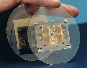
Silicon-on-sapphire IC mounted on sapphire wafer
Stacked two 3" sapphire wafers. 0.001" line, 0.001" space, with integrated decoupling capacitor, and integrated active substrate in 1982, using specially developed sputtered fluxless hermetic interconnect.
 |
 |
| Wafers before stacking | Close up |
This product was designed using liquid Helium design rules.
Particle Interconnect - Hughes Aircraft 1988 joint venture in Known-Good-Die
Resulting in a supercomputer assembled with Known-Good-Die in 2" x 4" x .1".
Science/Scope 1989 Hughes Aircraft Company:
"A new technique for packaging large-scale integrated circuit (IC) chips will permit much denser packaging on the substrate than previously possible. High-density multichip interconnect (HDMI) technology, being developed by Hughes, is designed to meet the needs of the next generation of VHSIC II hybrid circuits, which require dense packaging with no signal degradation at frequencies over 100 MHz. HDMI packaging achieves these results using a multi-layer substrate, a polymer dielectric highly suited to fine line metallization processing, and lithography techniques capable of producing 10-micron line widths. The technology is expected to be used in radar, sensing, tracking and guidance programs."
"The Data Memory Structure (DMS) multichip module is a very high speed cache memory system, switchable at high speed, to either of 3 input or output ports."
"HDMI can accommodate six 129K gate arrays (.640x.640 mil/die, 550+ pads/die; total 750,000 gates and 3,300 pads), 52 capacitors, and 24 - 15 nsec SRAM (32+ pads/die; total 750+), interconnected (using 70+ mil wire bond alleys) on a 2" x 4" = 8 in2 substrate having 368 I/O's."
"Performance of high speed circuits is also enhanced with low K polyimide dielectric used in the HDMI multilayer thin film (solder sealed ceramic leaded package) structure."
(All components tested/burned-in/speed sorted using PI resulting in 15+% yield improvement over production parts. Die price set at $5,000@ x 6 = $30,000, therefore DMS price >$100,000@)
PI's proposed removable die MCM-L/D/C to Hughes Aircraft.
Proposed to purchased a wafer for a total of $1,000 which was comprised of 300 die (5K gates/die .275 x .275 in.2/die, 180 pads/die for a total of 1,500,000 gates and 54,000 pads) interconnected on a 4" x 6" = 24 in.2 substrate. 50 mil pitch array yielded up to 9,600 I/O's.
Cost is further reduced by common low K polyimide multilayer PCB using 6+ mil pitch traces.
Environmental sealing of each die would also produce better reliability and upgradeability.
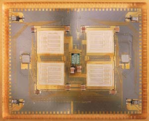
Particle Interconnect - Hughes 1989 Fire Finder MCM

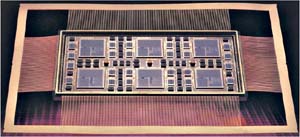
Particle Interconnect - Sandia Lab mBGA KGD packaging solution
For multichip modules and chip on board.


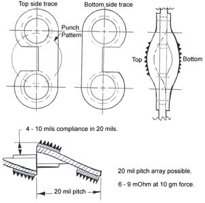
Flex circuit interposers
| Connecting two die. | Connecting several die. |
 |
 |
| 0.030" pitch 19x19 miniBGA socket. | 0.050" pitch, 15x15 through-hole BGA socket. |
Description
Description
Particle Interconnect replaces soldering, wire bonding, and on-bump bonding with environmentally safe, diffusion bonding at very low contact force, and no wiping.
Bonding temperature can vary from -270° C to > 450° C, allowing to minimize thermal stress due to CTE mismatch. Mono-metallic bonds (Particle Interconnect) unlike bi-metallic ones (solder) do not decay over time, due to temperature.
Particle Interconnect is the ultimate technology in electrical / mechanical / thermal interconnection with best price and best performance (not just price/performance) compared to other interconnect technologies.
Particle Interconnect is the only interconnect method with lead length of 0.001" (25 μ), bandwidth > 100 GHz, and a lifetime of > 1.5 million insertions, with extreme acceleration tolerance.
This unique technology creates an oxide penetrating, non-wiping gas tight connection that allows electrical connection in presence of adhesive, oil, and dirt.
Eliminating wirebonding, PCB drilling, and reducing PCB blind vias leads to device miniaturization by more than an order of magnitude, with reduced power needs and costs, through the use of MCM or SIP.
Because of reduced process steps and reduced material costs, the interconnect cost half the current industry practices. Additionally, mounting these connection points is faster, easier, and requires little specialized equipment or skilled labor.
Features
- Temporary, or permanent contact even in presence of adhesive, grease, or solder.
- Minimal disturbance of contact mating surface.
- Simple mechanical connection and trace design.
- Gas-tight oxide-penetrating connection.
- Plastic deformation of contact mating surface.
- Independent of common electronic metals.
- Contact material: nickel, gold, copper, ...
- Substrate material: polyimide, FR-4, ceramic, ...
- Temperature range used: > 450° C; to -270° C.
- Minimum interconnect dimensions: 6 μ pad, 12 μ pitch.
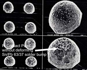
- Attached die passed four cycles of Mil-Std-883C (burn-in, thermal shock, pressure, salt/fog corrosion) test without any damage.
- No lead, see: U.S. Environmental Protection Agency - Design for the Environment (DfE) - Solders in Electronics: A Life-Cycle Assessment
- Life test: at 30 gram-force produced 3 - 5 milli-Ohms contact resistance even after 1,500,000 insertions, because metal matrix binding the particles is elastic and does not creep.
- Contact force & resistance:
- 10 gram-force, 10 milli-Ohms of resistance,
- 50 gram-force, 3 milli-Ohms of resistance.
- Current carrying capability: 0.020"2 pad at 9 gram-force has > 12 amps.
- Vertical axis contact length (signal integrity requires small size): 0.001" (25 μ).
- Vertical axis compliance (accomodating non-planar die): > 0.040" (depending on design).
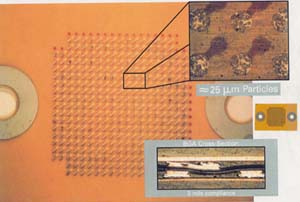
- Method for penetrating the oxide of package lead: sharp small diamond particles with no scrubbing for durability, compared to metal scrubbing or metal penetrating contacts.
- Controlled impedance: 50 Ω ± 1 Ω to the lead of package (Typical design capacitance & inductance: < 0.001 pF & < 0.01 nH).
- Bandwith tested to > 65 GHz (for high-speed and radio-frequency applications).
- All steps of electronic product development: prototyping, test (controlled impedance), burn-in, emulation/characterization, field replacable, and production.
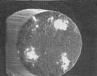
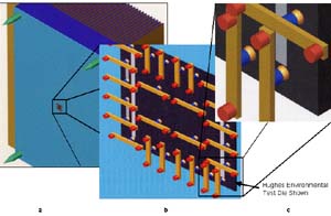
Particle Interconnect - Hughes environmental test die
Particle Interconnect removable MCM die socket.
100% of 500 die lot survived 4x Mil-Std-883C.
- Particle Interconnect with both adhesive and mechanical hold-down of chips while accumulating 4 runs of:
- 168 hours (672 hours total) 125 ° C for burn-in (other test passed are continuous 125 ° C),
- 500 cycles (2,000 cycles total) -55 to +125 ° C fast ramp MIL-STD-883C shock test,
- 24 hours (96 hours total) in salt/fog corrosion test,
- 24 hours (96 hours total) HAST (Highly Accelerated Stress Testing) pressure chamber (30 psi, +125 ° C pressure pot),
- Results in 50,000 die lot test prior to transfer into production.
- 96/4 Pb/Sn reflowed plated bump to spherize with special passivation configuration.
- Die orientated same as CAD picture for clarity (see: Removable die MCM - L/D/C).
- Note contact resistance test pads on left edge.
- Note traces for passivation crack detection.
- Note temperature sensors in center of die.
- Note traces for edge crack detection.
- Note traces for die heating.
- Note Particle Interconnect imprint.
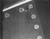
Particle Interconnect - Sandia Lab Known Good Die (KGD)
Known-Good-Die probe/burn-in. Proof of removable die MCM-L/D/C.
- 0.030" pitch 19x19 miniBGA.
- Burn-in at 125 ° C, 168 hours.
- 0 failures, 100+ runs, no deformation.
 |
|
| 0 failures, 11 runs shown above. | Particle Interconnect surface mount BGA socket. |
 |
 |
| Particle Interconnect - Sandia mBGA interposer schematic. | Sandia mBGA interposer |
Particle Interconnect - Hughes Aircraft 1988 - 1989
50,000 die joint production test venture.
Before burned-in:
- No bump deformation.
- Die Sn/Pb 3/97, socket Au 100, load 1 gm/mil2 pad to socket. Burned-in 125 ° C for 168 hours. Particles milled into gold ceramic ink and fired onto ceramic substrate. (Depression in center of bump is aluminum die pad covered by protective passivation layer.)
 |
 |
| 50x bumped chip before pressing against PI gold thick film. | 500x bump before contacting PI. |
After burned-in:
- No bump deformation.
- PI/gold bonded to tin/lead bump and was ripped off substrate. Resulting in using nickel as higher strength Particle Interconnect bond layer in future test socket/temporary contact usages and other metal combinations in permanent usages.
 |
 |
| 50x bumped chip after pressing against PI gold thick film metal matrix with 1 gm/mil2 load. | 500x bump after contacting PI, metal matrix is on bump. |
Packaging
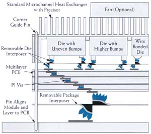
Removable die Multichip Module - L/D/C
|
|
 |
 |
| Removable die MCM | Louver contact |
- Low-cost heat exchanger designed for modular dissipation needs.
- Removable die locator (precisor) aligns all die on 0.010" edge-to-edge mosaic tile pattern of silicon.
- Precisor is accurately aligned by corner guide pins in heat sink.
- Removable die PI interposer sockets die to PCB and spring loads die against heat sink.
- Interposer is accurately aligned by corner guide pins in heat sink.
- Removable die PI interposers with 0.001" - 0.008" travel on 0.001" - 0.030" pitch are available.
- Removable multilayer PCB interconnects all die together with controlled impedance from die pad to die to pad.
- PI vias between laminate layers allow 0.002" "blind" vias by punching through adhesive layer during lamination.
- PCB is accurately aligned by corner guide pins in heat sink.
- Removable package PI interposer sockets package to PCB and spring loads package to PCB.
- MCM is accurately aligned and held to PCB by corner guide pins for manual or automatic insertion.
- Package interposers with 0.08"-0.020" travel on 0.010"-0.050" pitch with either peripheral or array patterns available.
- Die are removable by simply unstacking layers.
- Both bumped and wire bond die pads are mixable.